|
|
Spring 2012 Seminars
|
|
Title : Simplified current-steering DAC design for lower power and increased settling time using half rate clocking
Speaker: Dr. Bob Schell, Analog Devices, Inc.
Date: Friday, Feb 3rd, 2:00pm, Room 633 Mudd
Title : Synthesizing accurate clocks with inaccurate components
Speaker: Prof. Pavan Kumar Hanumolu, Assistant Professor, Oregon State University
Date: Friday, Feb 10th, 2:00pm, Room 633 Mudd
Title : Statistical SPICE Modeling Using Backward Propagation of Variance (BPV)
Speaker: Dr. Colin McAndrew, Freescale Semiconductor, Inc.
Date: Thursday, Feb 16th, 2:00pm, Interschool Lab (CEPSR 750),
Title : Neuromorphic Chip Design with a Scalable Architecture for Learning in Networks of Spiking Neurons
Speaker: Dr. Jae-sun Seo, IBM
Date: Friday, Mar 2nd, 2:00pm, Room 633 Mudd
Title : Interferer Robust Wide-band Receiver Techniques (EDS/SSCS Distinguished Lecture)
Speaker: Prof. Bram Nauta, University of Twente, Netherlands
Date: Friday, Mar 9th, 3:00pm, Interschool Lab (CEPSR 750)
Title : Large-scale EM simulation for RF IC design
Speaker: Dr. Sharad Kapur,, President, Integrand Software Inc.
Date: Wednesday, March 14th, 2:00pm, Room 633 Mudd
Title : High Data Rate Analog to Digital Conversion for Wired/Wireless Communication Systems
Speaker: Dr. Mihai Sanduleanu, IBM
Date: Friday, March 30th, 2:00pm, Room 633 Mudd
Title : Prospects of Semiconductor on Insulator (SOI) Technology in Power Amplifiers and Integrated Nanoelectromechanical Systems
Speaker: Prof. Saeed Mohammadi, Purdue University
Date: Friday, April 6th, 2:00pm, Room 633 Mudd
Title : Activities in passive and active submm-wave imaging at VTT / MilliLab
Speaker: Dr. Arttu Luukanen,
Research Professor, Micro
and Nanosystems
VTT Technical Research
Centre of Finland,
Director, Millimetre Wave Laboratory of Finland
Date: Wednesday, May 2nd, 1:30pm, EE conference room, 1300 Mudd
Title : From Microwave to Millimeter-wave: The Design of Reconfigurable, High-Bandwidth CMOS Radios
Speaker: Prof. Jeyanandh Paramesh, Carnegie Mellon University
Date: Friday, June 1st, 2:00pm, Room 633 Mudd
Title : Time-domain ADCs for Digital-Intensive RF Receivers and Health-care ICs for Non-electrical Vital Sign Monitoring
Speaker: Prof. Seonghwan Cho,
Korea Science Academy of KAIST, South Korea
Date: Thursday July 12th, 2pm, 633 Mudd
|
|
|
|
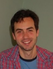
Dr. Bob Schell
Analog Devices, Inc.
Date:
February 3rd, 2:00pm
Location:
Room 633 Mudd
|
Simplified current-steering DAC design for lower power and increased settling time using half rate clocking
Abstract:
Digital to analog converters have found their way into a variety of applications from static control loops, offset adjustments, baseband signal synthesis and increasingly for direct RF signal synthesis. As the output signal frequency increases, the DAC aspect that limits spectral performance (distortion) changes, bringing up new design goals. This talk starts by discussing DAC designs for DC to low frequency output signals and moves on to discuss design goals for high output frequencies. In this vein I present a new technique targeted at alleviating incomplete settling issues for high speed DACs, utilizing half rate clocking of a quad switch. By halving the frequency, the settling time allowed for clocks at the switches (as well as signals within the whole datapath) is doubled, reducing data dependencies for improved performance.
Biography:
Bob Schell received his BSE from Princeton University and his MS and PhD degrees from Columbia University. He has worked as a product engineer for MultiLink Technologies and Vitesse Semiconductor and as a design engineer for Conexant. He is currently a senior mixed signal designer working for Analog Devices in NJ. His interests are in both analog-to-digital and digital-to-analog converter design as well as serial high speed serial interfaces required by both of these blocks.
|
|

Prof. Pavan Kumar Hanumolu
Assistant Professor
Oregon State University
Date:
February 10th, 2:00pm
Location:
Room 633 Mudd
|
Synthesizing accurate clocks with inaccurate components
Abstract:
Generating precise clocks using clumsy transistors available in highly-scaled CMOS technologies is a challenging task. In this talk, several architectural- and circuit-level techniques that seek to overcome the detrimental impact of analog circuit imperfections that plague conventional clock generators will be discussed. After a brief overview of the drawbacks of classical analog phase-locked loops (PLLs), the talk progresses with the evolutionary presentation of highly digital clock generators. Several case studies of digital PLLs that achieve sub-ps absolute jitter, better than 1mW/GHz power efficiency and very wide operating range will be presented. Application of digital PLLs for supply noise cancellation and charge recycling will be outlined.
Biography:
Pavan Kumar Hanumolu received the Ph.D. degree in electrical engineering from Oregon State University in 2006. Currently, he is an Assistant Professor in the School of Electrical Engineering and Computer Science at the same University. His research interests include high-speed I/O interfaces, digital techniques to compensate for analog circuit imperfections, time-based signal processing, and power-management circuits.
|
|
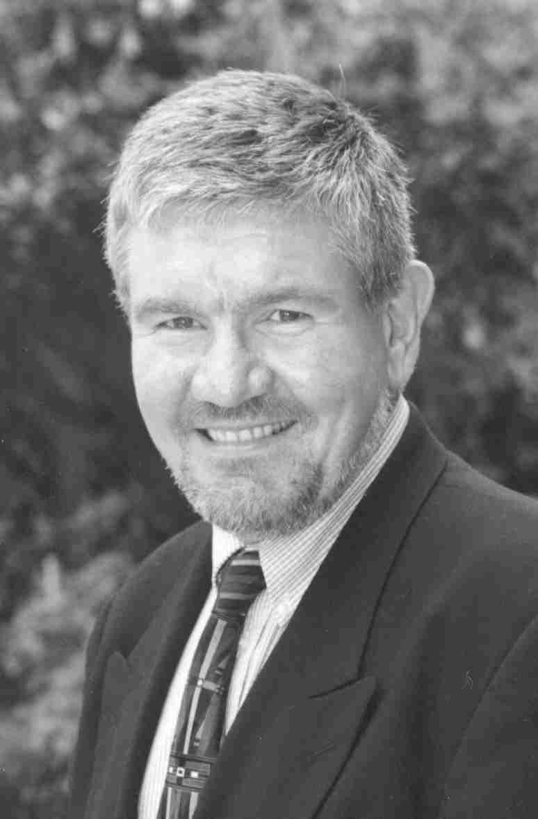
Dr. Colin McAndrew
Freescale Semiconductor,
Tempe, AZ
Date:
February 16th, 2:00pm
Location:
Interschool Lab(CEPSR 750)
|
Statistical SPICE Modeling Using Backward Propagation of Variance (BPV)
Abstract:
A key factor in IC design is to be able to determine the expected manufacturing variations that will arise in key measures of the electrical performance of circuits. This requires accurate statistical circuit simulation models. The different types of statistical models that are required for different types of statistical circuit analyses will be reviewed (including distributional models, corner models, and mismatch models), and the advantages and disadvantages of common approaches to generating these models will be discussed. The backward propagation of variance (BPV) technique will be covered in detail, showing that it almost "cheats" by force-fitting a model to give the desired results. Extension to handle explicit fitting of correlations will be covered, and it will be shown that circuit variations, as well as device distributions, can be included in the BPV modeling process.
Biography:
Colin McAndrew received the Ph.D. and M.A.Sc. degrees in Systems Design Engineering from the University of Waterloo, Waterloo, Ontario, Canada, and the B.E. (Hons) degree in Electrical Engineering from Monash University, Melbourne, Victoria, Australia. From 1987 to 1995 he was at AT&T Bell Laboratories, Allentown PA. Since 1995 he has been with Freescale Semiconductor (formerly Motorola), in Tempe AZ. His work is primarily on compact and statistical modeling and characterization for circuit simulation, for MOS transistors, bipolar transistors, and passives, and he has been a primary advocate of the use of Verilog-A and compilers for compact modeling. He was a recipient of the Ian Langlands Medal from the Institute of Engineers of Australia in 1978, best paper awards for ICMTS in 1993 and CICC in 2002, and the BCTM Award in 2005. He is a Fellow of the IEEE, was an editor of the IEEE Transactions on Electron Devices, and is or has been on the technical program committees for the IEEE BCTM, ICMTS, CICC, and BMAS conferences.
|
|
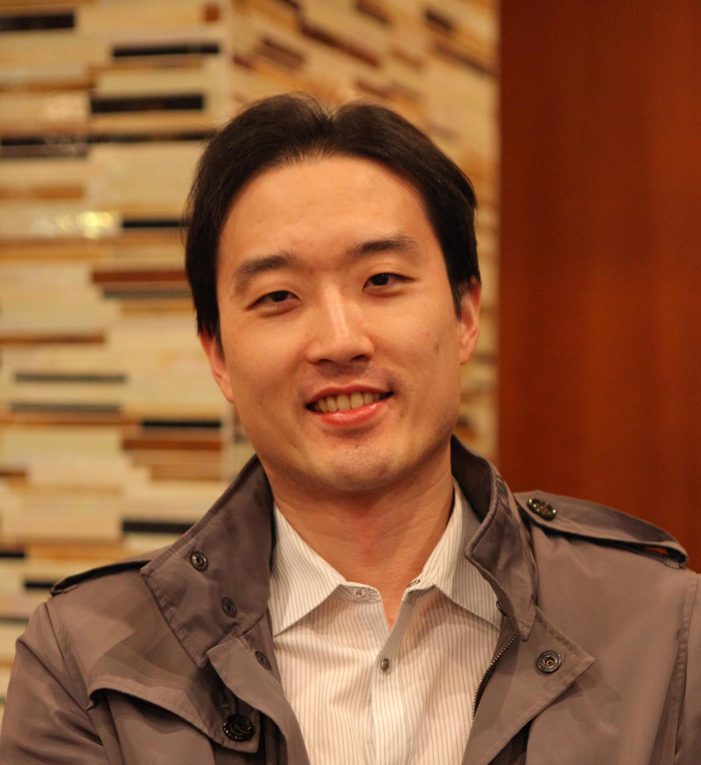
Dr. Jae-sun Seo
IBM T. J. Watson Research Center
Date:
March 2nd, 2:00pm
Location:
Room 633 Mudd
|
Neuromorphic Chip Design with a Scalable Architecture for Learning in Networks of Spiking Neurons
Abstract:
We present a scalable integrated circuit platform for networks of spiking neurons. The proposed platform incorporates (a) robust digital neuron circuits that exploit CMOS scaling; (b) novel transposable SRAM arrays that share learning circuits; and (c) crossbar fan-out for efficient on-chip inter-neuron communication. Through tight integration of memory (synapses) and computation (neurons), a highly configurable chip comprising 256 neurons and 64K binary synapses with on-chip learning based on spike-timing dependent plasticity is demonstrated in 45nm SOI-CMOS. Near-threshold, event-driven operation at 0.53V is demonstrated to maximize power efficiency for real-time pattern classification, recognition, and associative memory tasks. Future scalable systems built from the foundation provided by this work will open up possibilities for future brain-like computing systems.
Biography:
Jae-sun Seo received the B.S. degree in electrical engineering from Seoul National University, Korea, in 2001, and the M.S. and Ph.D. degree in electrical engineering from the University of Michigan in 2006 and 2010, respectively. As a graduate student, he has worked at Intel circuit research lab and Sun Microsystems VLSI research group, exploring new circuit designs for on-chip communication in microprocessors. In 2010, he joined IBM T. J. Watson Research Center, where he is presently a research staff member, working on energy-efficient integrated circuits for high-performance and low-power VLSI systems. Mr. Seo was a recipient of Samsung Scholarship from 2004 to 2009.
|
|
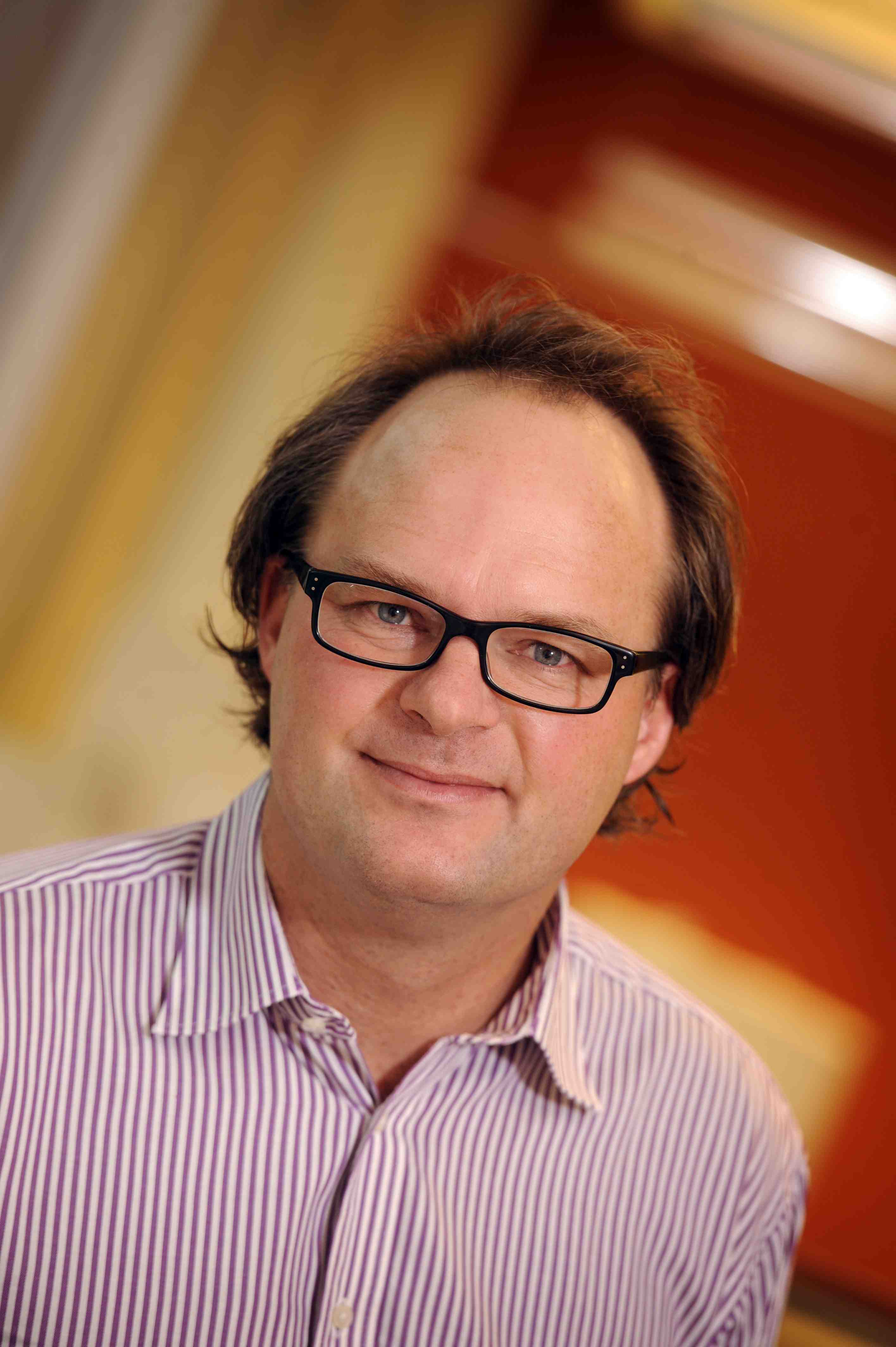
Prof. Bram Nauta
University of Twente, Enschede, The Netherlands
Date:
March 9th, 3:00pm
Location:
Interschool Lab(CEPSR 750)
|
Interferer Robust Wide-band Receiver Techniques (EDS/SSCS Distinguished Lecture)
Abstract:
Software defined radios are radios which can send and receive according to many standards with one piece of hardware. This hardware can be configured by software and is preferably integrated in an IC. Challenges in this type of radio are: wide band RF operation or wide-RF band tunable operation. This means that RF filtering is relaxed and in turn this makes the robustness to interference a great challenge. In this presentation several techniques will be given to increase interference robustness. Key ideas are presented in: Avoiding voltage gain at RF, 2-step harmonic rejection technique and a translational loop feedback receiver. Also a revival of N-path filters is presented, which allow tunable, linear and low-noise high-Q filters at GHz frequencies in standard CMOS.
Biography:
Bram Nauta was born in Hengelo, The Netherlands. In 1987 he received the M.Sc degree in electrical engineering from the University of Twente, Enschede, The Netherlands. In 1991 he received the Ph.D. degree from the same university on the subject of analog CMOS filters for very high frequencies. In 1991 he joined the Mixed-Signal Circuits and Systems Department of Philips Research, Eindhoven the Netherlands. In 1998 he returned to the University of Twente, as full professor heading the IC Design group. His current research interest is high-speed analog CMOS circuits.
He served as Associate Editor of IEEE Transactions on Circuits and Systems –II (1997-1999). He was Associate Editor (2001-2006) and later the Editor-in-Chief of IEEE Journal of Solid-State Circuits (2007-2010). He is the 2013 Chair of the technical program committee of the International Solid State Circuits Conference (ISSCC) . Moreover, he is member of the technical program committee of the European Solid State Circuit Conference (ESSCIRC), and the Symposium on VLSI circuits. He is co-recipient of the ISSCC 2002 and 2009 "Van Vessem Outstanding Paper Award", is distinguished lecturer of the IEEE, member of IEEE-SSCS AdCom and IEEE fellow.
|
|

Dr. Sharad Kapur
President, Integrand Software Inc.
Date:
March 14th, 2:00pm
Location:
Room 633 Mudd
|
Large-scale EM simulation for RF IC design
Abstract:
Accurate modeling of passive components and passive component ensembles is a critical
step in high-speed design. In this talk, we will discuss some of the recent enhancements
in our full-wave 3D electromagnetic simulator EMX. We discuss the various simulation
and design issues that arise in the modeling of passive structures, such as, handling
density dependent effects at sub 40nm nodes, simulation of 60GHz circuitry, modeling of
thru-silicon-vias and the creation of scalable models for components. EMX is being used
for simulation and modeling of a wide class of passive circuits including spiral inductors,
MIM/MOM capacitors, Baluns, Filters, VCOs and RF Blocks and circuit ensembles.
Several designs, fabricated on a variety of process technologies ranging from 0.25um to
28nm CMOS, SiGe and high-resistivity substrates, will be presented with comparisons to
measurement.
Biography:
Dr. Sharad Kapur is the president and co-founder of Integrand Software, Inc. He
graduated with a Ph.D. in Computer Science (Numerical Analysis) from Yale University
in 1996. He joined Bell Labs in 1996 as a member of technical staff. While at the design
automation group at Bell Labs he co-developed several large software packages and
tools, for electromagnetic analysis, circuit simulation and chip-level extraction. In 2003
he co-founded Integrand Software, Inc and helped develop the EMX 3D EM simulator.
He is the author of over 30 peer-reviewed publications, primarily in the area of numerical
analysis and electronic design automation. He is the holder of 6 US patents.
|
|

Dr. Mihai Sanduleanu
IBM T. J. Watson Research Center
Date:
March 30th, 2:00pm
Location:
Room 633 Mudd
|
High Data Rate Analog to Digital Conversion for Wired/Wireless Communication Systems
Abstract:
Future Long Haul optics and high-density chip-to-chip I/O communication systems would require nonlinear equalization in the digital domain.
With technology scaling and less analog options in modern CMOS technologies there is a clear evolution path towards ADC-DSP centric
wired/wireless communication systems. The talk will address the design challenges and calibration techniques for high data rate ADCs
realized in CMOS SOI technologies from IBM. Design trade-offs will identify fundamental limits and voltage domain / time domain analog-to-digital
converter systems are discussed with their advantages and shortcomings.
Biography:
Mihai Sanduleanu received the MSc degree in electrical engineering from "Gh. Asachi" University, Iasi, Romania in 1990 and the MEE degree from Eindhoven International Institute, Eindhoven, The Netherlands in 1994. In 1998 he received the PhD degree from University of Twente, Enschede, The Netherlands. In 1998 he joined the Fiber Optics Communication group from Philips Semiconductors, Nijmegen, The Netherlands. From 2000 until 2007 he conducted research on RF, mm-Waves and Fiber Optics communication circuits at Philips Research Eindhoven. From 2006 until 2007 he was part-time Professor at Eindhoven University of Technology, Eindhoven, The Netherlands in the Microelectronics Department. From 2008, he joined the Communication and Computation Department of IBM T.J. Watson Research Center. His current research interest is in high-speed analog CMOS circuits, mm-Waves and sub mm-Waves circuits.
He is Associate Editor of IEEE Transactions on Circuits and Systems and member of the technical program committee of the Custom Integrated Circuits Conference (CICC).
|
|
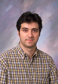
Prof. Saeed Mohammadi
Associate Professor, School of Electrical and Computer Engineering, Purdue University
Date:
April 6th, 2:00pm
Location:
Room 633 Mudd
|
Prospects of Semiconductor on Insulator (SOI) Technology in Power Amplifiers and Integrated Nanoelectromechanical Systems
Abstract:
Silicon on Insulator (SOI) technology has been widely used for low power analog and digital circuits for applications in mobile computation and communication. An addition of a buried oxide layer beneath a thin Si device layer in SOI technology brings about a new physics to the CMOS transistor, one that is still not fully understood. The buried oxide layer reduces the parasitic capacitance of transistors and interconnect metallizations to the Si substrate, which in turn reduces the dynamic power dissipation. Moreover, the buried oxide layer, when combined with trench oxide, helps electrically isolate CMOS transistors from each other and from the Si substrate. Electrically isolated SOI transistors can be stacked on top of each other to form power amplifiers with large output voltage swings. On the other hand, buried oxide layer facilitates micromachining of thin Silicon Nanowires that can be easily made into suspended double-clamped nanoelectromechanical resonators. With excellent control over the fabrication process, these mechanical resonators are made reliable, reproducible and widely tunable. In addition, they can be excited in their nonlinear dynamics modes including parametric amplification and resonance modes. In this presentation, SOI applications in both power amplifiers and integrated Nanoelectromechanical systems are revisited and our most recent results are presented.
Biography:
Saeed Mohammadi graduated with a Masters degree in Electrical Engineering from the University of Waterloo, ONT, Canada in 1994. He earned his PhD degree in Electrical Engineering from the University of Michigan in Ann Arbor in 2000. Since 2002, he has been at Purdue University where he currently serves as an Associate Professor. His research interests are in the areas of experimental nanotechnology and RF circuits. Together with his students, Prof Mohammadi has published more than 120 papers in these areas including the first carbon nanotube RF transistor, the first transparent flexible display technology based on carbon nanotube thin film transistors and the first RF CMOS receiver implemented in subthreshold regime.
|
|
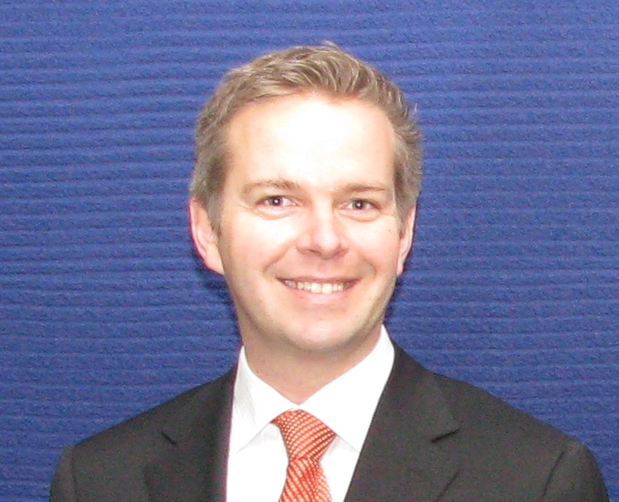
Dr. Arttu Luukanen
Research Professor, Micro
and Nanosystems
VTT Technical Research
Centre of Finland,
Director, Millimetre Wave Laboratory of Finland
Date:
Wednesday, May 2nd, 1:30pm,
Location:
EE conference room, 1300 Mudd
|
Activities in passive and active submm-wave imaging at VTT / MilliLab
Abstract:
Both active and passive submillimetre-wave stand-off imaging systems are under development for security imaging applications. The drivers for operation at higher frequencies have been the desire for better image resolution, smaller optics package, reduced susceptibility to specular reflections from the human skin and capability for stand-off imagery. In the talk I summarize our efforts on devices, components and systems which could eventually pave the way for fast, real time, high-resolution imaging systems for the submillimetre-wave range.
Biography:
Arttu Luukanen (born 1972, native of Finland) received his M.Sc. degree from the University of Helsinki, Finland in applied physics in 1999. He was awarded a Ph.D. in 2003 from the University of Jyväskylä, Finland, also in applied physics.
Dr Luukanen’s professional career began as a research assistant at Metorex International Oy, a Finnish company specializing in analytical X-ray instruments for the metal industry and a supplier of X-ray detectors for several space science missions of the European Space Agency ESA, NASA, and NASDA. In 1996, Arttu Luukanen began investigating technologies for passive millimeter wave imaging for concealed weapons detection. This research culminated in passive scanned imagery of objects taken with an imaging system utilizing antenna-coupled microbolometers as the detectors. Dr Luukanen continued his bolometer research as a graduate student at the University of Jyväskylä, Department of Physics under a joint ESA contract with Metorex. His Ph.D. research focussed on the development of ultra-sensitive transition-edge microcalorimeters and microbolometers for X-ray and THz sensing applications. After completing his Ph.D., Dr Luukanen took a research scientist position at VTT Technical Research Centre of Finland. From 2003 to 2005 he worked as a guest researcher at the National Institute of Standards and Technology in Boulder, Colorado (USA), developing an active millimetre-wave imaging system based on antenna-coupled microbolometers. In 2005, Dr Luukanen was nominated as the Director of MilliLab, the Millimetre Wave Laboratory of Finland (www.vtt.fi/millilab). Since 2006, Dr Luukanen has served as the chairman of IEEE Electron Devices/Microwave Theory & Techniques and Antennas & propagation Chapters of the IEEE Finland Section.
|
|

Prof. Jeyanandh Paramesh
Carnegie Mellon University
Date:
June 1st, 2:00pm
Location:
Room 633 Mudd
|
From Microwave to Millimeter-wave: The Design of Reconfigurable, High-Bandwidth CMOS Radios
Abstract:
From Microwave to Millimeter-wave: The Design of Reconfigurable, High-Bandwidth CMOS Radios
The first part of this talk describes the application of phase-change vias to reconfigure CMOS integrated circuits. CMOS-compatible phase-change materials feature high contrasts in resistivity between the amorphous and crystalline states. While this property is being exploited in an emerging class of non-volatile memories, we are exploring its utility as a technological element to reconfigure integrated circuits, especially analog and RF circuits. The development of CMOS-compatible reconfigurable inductors, their application in a reconfigurable LC-VCO, as well as the underlying material choices and integration techniques are discussed. Other reconfigurable CMOS circuits including a low-offset comparator and a non-volatile look-up table are described. Characterization results from prototype circuits are presented to validate these concepts.
The second part of this talk addresses the design of low-power millimeter-wave radios in CMOS with extremely wide bandwidths. The mm-wave frequency bands hold enormous potential for multi-Gb/s communications as well as emerging imaging and ranging applications. The realization of this potential will be underpinned by the development of high-performance, power-efficient transceivers in nanoscale CMOS technologies. Two key challenges must be met towards achieving this goal. First, the mm-wave front-end circuits must be designed to operate over extremely wide bandwidths of several tens of GHz, both to exploit the large bandwidth availability, and also to provide sufficient margins to tolerate process, voltage and temperature variations that are increasingly problematic in nanoscale CMOS. Second, reducing power consumption in the front-end is imperative especially since phased-arrays are mandated in mm-wave transceivers.
This latter half of this talk describes our recent work towards achieving these goals. Transformer-based unilateralization techniques are introduced to enable the design of low-noise amplifiers that achieve over 10 GHz of bandwidth and can operate from a scalable power supply from the nominal voltage down to very low voltages. Low-voltage, ultra-wide bandwidth receivers for pulse-based mm-wave signals, and phased-array receivers, based on the aforementioned amplifiers, are presented. The design of transformer-based voltage-controlled oscillators with several 10's of GHz of tuning range is then described. Results from the characterization of several test circuits in 130 nm and 45 nm CMOS technologies are presented.
Biography:
Jeyanandh Paramesh received the B.Tech, degree from IIT, Madras, the M.S degree from Oregon State University and the Ph.D degrees from the University of Washington, Seattle, all in Electrical Engineering. He is currently Assistant Professor of Electrical and Computer Engineering at Carnegie Mellon University. He has held product development positions with Analog Devices, where he designed high-performance data converters, and Motorola where he designed analog and RF integrated circuits for cellular transceivers. From 2002 to 2004, he was with the Communications Circuit Lab, Intel where he developed multi-antenna receivers, high-efficiency power amplifiers and high-speed data converters high data-rate wireless transceivers. His research interests include the design of RF and mixed-signal integrated circuits and systems for a wide variety of applications.
|
|

Prof. Seonghwan Cho
Korea Science Academy of KAIST, South Korea
Date:
July 12th, 2:00pm
Location:
Room 633 Mudd
|
Time-domain ADCs for Digital-Intensive RF Receivers and Health-care ICs for Non-electrical Vital Sign Monitoring
Abstract:
In the first part of the talk, a time-domain ADC using voltage-controlled oscillators will be presented for a digital-intensive direct RF sampling receiver. Unlike conventional delta-sigma band-pass ADCs that require high speed analog circuits and passive components, the proposed architecture provides band-pass function by time-interleaving 1st-order noise-shaped VCO-based ADCs. The use of VCO-based ADC has the advantage that its resolution is determined by time-resolution rather than the voltage resolution, thus making it attractive for future low-voltage CMOS processes. In the second part of the talk, a technique to monitor pulse-wave velocity and respiration will be presented. By exploiting the change of electrical impedance in human body, we will show that such non-electrical vital signs from human body can be measured in an all electrical way.
Biography:
SeongHwan Cho received the B.S. degree in electrical engineering from KAIST, Korea, in 1995, and the S.M. and Ph.D. degrees in EECS from MIT, Cambridge, MA, in 1997 and 2002, respectively. In 2002, he joined Engim, Inc., where he was involved in data converters and phased-locked loop (PLL) design for IEEE 802.11abg WLANs. Since November of 2004, he has been with KAIST in the department of EE, where he is now an associate professor. His research interests include mixed-signal and analog circuits for low power communication systems and bio/health-care devices. Prof. Cho was the co-recipient of the 2009 IEEE Transactions on Circuits and System Society Guillemin-Cauer Best Paper Award. Prof. Cho serves on the technical program committee on several IEEE conferences, including ISSCC, Symp. on VLSI and A-SSCC. He has served as an associate editor of IEEE Transactions on Circuits and Systems-I and a guest editor of JSSC.
|
|
|

