We have access to a number of different semiconductor processes for the fabrication of our circuits through a fabrication service provides (e.g., MOSIS, Europractice) as well as through direct relationships with companies and foundries. We currently mainly use 90nm CMOS, 0.13um CMOS, 0.18um CMOS and 0.25um/40GHz BiCMOS processes and are initiating our work in 65nm and 45nm CMOS processes. Take a look at our Chip Gallery!
We use a full set of industrial grade design tools for our IC designs. This includes tools suites from Cadence, Mentor and Agilent. We use PC desktops running Linux as well as servers running SunOS and Linux.
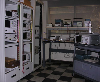
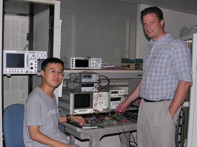
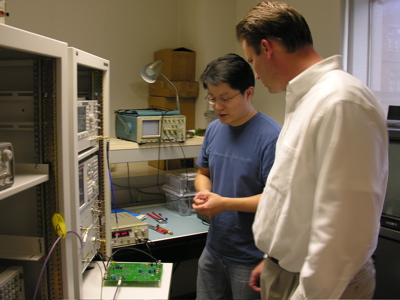
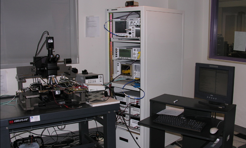
Our lab facilities went through a substantial upgrade during 2004 and 2005 thanks to an NSF MRI Grant (with Prof. Tsividis) in conjunction with funding from Columbia University and the School of Engineering. We currently have a state-of-the-art measurement facility for IC characterization from DC to 40 GHz. We can measure on wafer circuits or packaged devices. Our instruments allow a full characterization in the frequency domain and time domain.