
If you haven't read the CAD tool information page, READ THAT FIRST.
In this handout, we are going to learn the following :
This handout has two parts. In Part I you are to work through the schematic composer tutorial that comes with the cadence on-line documentation, called openbook.
In Part II, we will do a simple inverter layout simulation using HSPICE through cadence' Analog Artist environment.
Follow the steps :
/usr/cad/cds/tools/dfII/samples/tutorials/composer/tutorial
cp -pr /usr/cad/cds/tools/dfII/samples/tutorials/composer/tutorial .
Type openbook at the UNIX prompt to bring up the Cadence on-line documentation. Choose the "Design Entry" option from the main page. Then select "Virtuoso Schematic Composer Tutorial."
Please do the Cadence Composer tutorial, Chapters 2 - 5. Please use icfb& to bring up the Cadence software. It will take several hours to work through the tutorial, but it is worth it!. It is very important that you are familiar with Composer, so please don't cut
any corners here.
In this part we will draw a simple inverter in the schematci composer and then do a transient simulation using the Analog Artisit Environment of cadence. Follw the Steps :
Step1 :Invoke cadence by typing icfb &
Step2 :Click on Tools--->Library Manager....The library manager window should pop up soon.
Step3 :Click on File ---> New ---> Library .
Step4 :On the "New Library" window, give a new library name.
Step5 :A "technology file for new Library" window pops up. Click on don't need a techfile and click OK .
Step 6:Your library should now be listed in the library manager's "Library" section.
Step 7:In the library manager window, Click on the library you just created and choose File ---> New ---> Cellview .
Step 8:On the "new file" window, which popped up, give a new cell name (i'll call it mycell) . Make sure that the library name should be same as what you gave , view name should say "schematic" and tool should say "composer-schematic". If the "tool" shows something else, you can click on the button and choose "composer-schematic".
Step 9:Hit 'OK" and a schematic editing window pops up showing the library name, cell name (mycell) and view name which is "schematic" in this case.
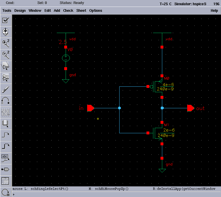
Step 10 : Now you are ready to draw a schematic in this window which will finally look as shown in the figure below. Look around for a few seconds and make yourself comfortable with the GUI. check out various options on the pop-down menus and also move your mouse over the toolbar on the left edge of the window for some most commonly used commands.
FIG 1.
Step 11: Now we will place the nmos and pmos for the CMOS inverter. Choose Add --> Instance . Give tsmc025 for the "library" , pmos for the "cell" and symbol for the "view". "Names" field should be blank. Notice that "bulk node connection" has vdd! in it (which is generally the case for a pmos) and length has 240.00n M". This is the smallest possible channel length for the TSMC technology which we are using. Fill 4u in the "width" and move your mouse over the schematic window. A pmos transistor symbol will follow your mouse pointer. Place the pmos device on the window and hit "Esc". Note : In cadence, whenever, you are in the middle of a command, hit "Esc" to end it.
Step 12 : Again choose Add --> instance and fill in similar to Step 11 except nmos in the "cell" and 2u as the "width". Note this time that the "bulk node connection" shows gnd! which is generally the case for nmos. Move your mouse over the schematic window and place the nmos transistor vertically below the pmos as in FIG 1 above.
Step 13:We will now place the "vdd" and "gnd" symbols. Choose Add --> instance . Fill "library" as analogLib , "cell" as vdd and "view" as symbol . Place it on your schematic just as you placed the transistors. Similarly place the "gnd" symbol by filling gnd for the "cell" in the "add instance" form.(look at FIG 1 for the position of vdd and gnd ).
Step 14: Now we will make wiring connections. choose Add --> wire (narrow) and click on the drain of pmos. A wire segment will follow your mouse. Bring the mouse pointer over the drain of nmos and click it to complete the wire section. Hit "Esc" on your keyboard to end the command. Similarly, draw all the wires shown in blue in fig 1. above.
Step 15: Put the pins "in" and "out" by choosing add -->pin and giving "in" and "out" for "Pin names" one by one. Make sure to choose "direction" as input for "in" and output for "out". Other options on the "add pin" form remain unchanged. Place the pins as shown in FIG 1.
Step16 : Finally we have to define our vdd as 2.5 volts. We do so by adding a dc voltage source as shown in the top left of FIG 1. Choose add --> instance and give "library" as analogLib , "cell" as vdc and view as symbol . Fill in the "DC voltage" field as 2.5v . Place the voltage source on your schematic and put the "vdd" and "gnd" symbols on it as described in Step 13 and as shown in fig 1.
Step17 :Congratulations! You have just completed your first schematic in Cadence. To check and save your design, click on the first icon to the left of the schematic (it is the icon with a box and a check mark). You will be warned if you have any floating wires or pins. You can also perform the same function by selectingCheck and Save from the Design menu of the schematic window. To close the schematic window, select Close from the Window menu in the schematic window.
Step 18: Now we will make a symbol for this schematic. From your Schematic Editing window, choose Design --> Create Cellview --> from Cellview... A new "Cellview from cellview" window pops up. Everything should be already set on this window by default. Make sure it looks as shown in Fig 2. Then just OK the form. Another "Symbol generation Options " window pops up. Just OK this window. Soon after a "Symbol Editing Window" pops up with a rectangular shaped symbol of an inverter (shown in FIG 3.). This doesn't REALLY look like an inverter symbol, but it doesn't matter for simulation. If you are really keen , you can modify this symbol using the graphic tools available on this window so that it really looks like an inverter symbol but thats not mandatory. Here is the detailed information for doing this.
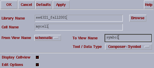
FIG 2.
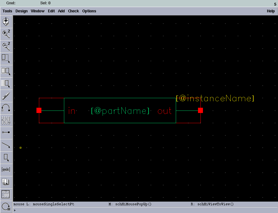
FIG 3.
Step 19: Close both windows (schematic and symbol) and click here to move on to the simulation part .