

1. For every cell that needs to be tested, we will need to generate
a test schematic. For an inverter, create another cell called 'inverter_test'
in your current library ( for the tutorial we assume that the current library
is 'ee4321_fall2001'). Create a schematic view for this
cell. Refer to " Cadence Schematic Composer Information " page for the tutorial on how to create a schematic.
For your convenience, the steps are mentioned again. Click on File
--> New --> CellView in the CIW window. Then enter Library Name
as ee4321_fall2001, cellname as inverter_test
and View Name as
Schematic. This should pop-up
an empty schematic creation window. In this window, you will generate a
schematic as shown below:
To generate a schematic like this, you will need to go through the following steps. This assumes that you already have an inverter schematic (we called it "mycell") and its symbol.
1 a. Place an instance of mycell by
pressing 'i'. ( how to place
an instance has already been discussed in " Cadence Schematic Composer Information" page).
Make sure that you choose
an inverter symbol from the ee560 library as your instance.
1 b. Place an instance for the piece-wise
linear voltage source (vpwl), which you can find in the analogLib
library and cell vpwl.
Enter it's properties using 'q'. The
vpwl source enables you to specify voltage source as a
piece-wise linear curve. Enter the voltages as discrete entries for different
time instants. The number of time instants is specified
by the number of pairs of points in the window below.

The above entry specifies voltage source at three points with (time,
voltage) values of (0,0) , (3us,0) and (3.001us,2.5) respectively.
In other words we entered a voltage source with a rise transition from
0 to 2.5V at 3us, with the rise time of 0.001us.
1 c. Place an instance of a capacitor,
which you can find under libraryAnalogLib and cell cap.
A capacitor will simulate the effect of capacitive loading from the
following stages. For illustration purposes, choose a value of 1pf
for the capacitor.
1 d. Place the ground gnd symbol as described on " Cadence Schematic Composer Information" page.
If you notice, we have created a test setup for the inverter, by giving it an input and having a capacitive load. Also notice that we described our power supply voltage to be 2.5 V in the inverter (mycell) schematic itself (see step 16 on " Cadence Schematic Composer Information" page). But if we wish, we can specify the power supply voltage here and skip the step 16 on " Cadence Schematic Composer Information" page
2. Now we will simulate this inverter using HSPICE in the cadence' analog artist environment. Re-open the inverter_test schematic window if you closed it. Choose Tools --> Analog Environment . You will see a window as shown below.
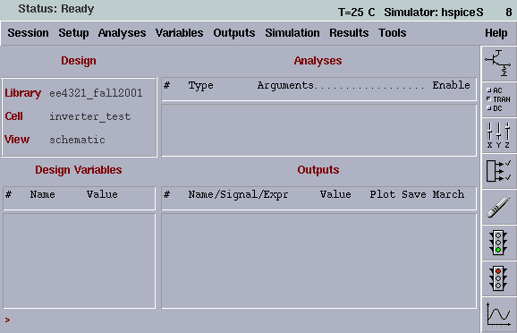
3. Choose Setup --> Environment.... An Environment Options window pops up. Click on hspice for "include/Stimulus file Syntax" and write /usr/tech/tsmc025/models/tsmctt in the "Include File" section. Everything else should be set by default. OK the form.
4. Choose Analyses --> choose... from the Analog Artist Simulation window (Shown above). You can perform either dc analysis which lets you sweep a dc voltage source or you can do transient analysis by choosing tran to observe the output as a function of time. ac and noise analysis is primarily used by analog designers to measure the frequency response and the noise performance of the circuit. In this tutorial we will focus on transient analysis. So, on the Choosing analyses window, click on tran and enter the time limits for simulation as shown below. Don't forget to choose Enabled at the bottom of the screen.
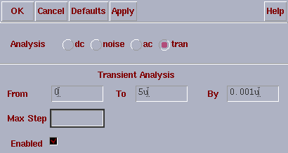
The above entries asks the circuit to perform transient simulation from 0 to 5us with a step of 0.001us or 1 ns.
5. Go to simulation menu in the Analog Artist Simulation window and click on Run. This will start simulation. ( It is important to understand what Cadence does, when you hit a Run. It first creates a raw netlist having just the top-level instances and the include files. Next it generates a final netlist by bringing in all transistor level details. And finally, it runs the Hspice simulation. You can also go through these steps manually, by first clicking on Simulation --> netlist -->Create Raw and then Simulation --> netlist --> Create Final and finally press Run. Every step will show you an intermediate netlist output for your review. If you just press Run the first and only time, it will do all the three in one step, without showing you the intermediate netlist output) .
This will start the simulation process.
6. The CIW window should show " Reading Simulation Data ...... Successful", to ensure that simulation was a success. If not go to Simulation --> Output Log in your Analog Artist Simulation window to find out what the problem was. Now you can still continue with Cadence to view your results, which is mentioned below or use "awaves" outside of cadence to view your results, not mentioned in the tutorial.
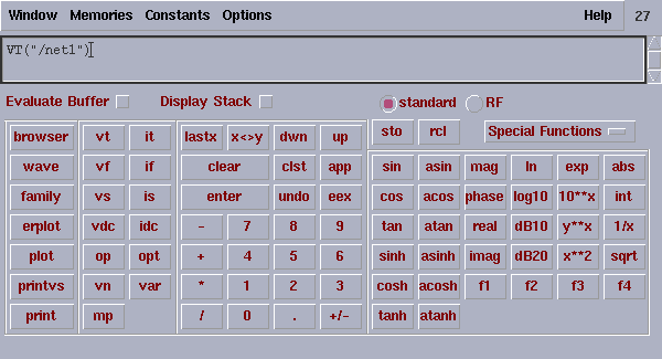
7. Go to Tools --> Calculator in the Analog Arstist Simulation Window. A very useful tool "Calculator" will pop-up. It is a very friendly and highly resourceful graphical user interface to view simulation results.
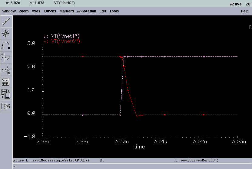
8. On the calculator, click on 9. Finally, if you plot the in and out nets of your inverter_test schematic, you will see the input and output Voltage Vs. time plots of your inverter with a load of 1pF of capacitance. It is shown in the window below. The white waveform shows the input to the inverter while the red one shows the output which as you can see is delayed due to tha finite capacitive loading.
Alternative Method
You can also use the cadence Analog Artist environment window just to give you a spice netlist. You can then use hspice in batch mode to do the simulation. for this, After Step 4 above, do the following :
1. Go to Simulation --> Netlist --> Create
Final in the Analog Artist Simualtion window.
2. Once the file is saved, open the file (filename.sp)
from the unix prompt using any text editor. You should see the following lines in your file.
.OPTION INGOLD=2 ARTIST=2 PSF=2
Now do the following:
a. Delete the .OPTION statement
from the file.
3. Once you have a complete updating your hspice file, run hspice in batch mode as described on the HSPICE and AWAVES Information page.
4. Finally, use awaves to view the plots as described on HSPICE and AWAVES Information page.
vt . This means you want to select a transient voltage on your schematic. When you click vt, you will see that your schematic window comes in front and has a small message at its bottom border saying >Select nets for VT expression. Now you click on one of the nets in your schematic window. You will see that the screen of your calculator shows the name of the net you just selected. Like , in above figure, I have "net1" selected . Now click plot on the calculator. A new Waveform window will pop up with a Voltage Vs. time plot of the net you selected. Select both the in and out nets of the inverter_test schematic and try to plot them. you need to hit "clear" on the calculator if it shows garbage.
A window will pop-up after few minutes.
This is the hspice netlist file of your schematic. Click on File
--> Save as in this window to save the netlist file with a .sp
extension (as in filename.sp ) in your run directory. It is
encouraged that you create a separate directory in your home directory
to save and run hspice simulations.
.PROBE=0
b. Add a
.option post statement instead.
THE END at last...