
Analog Circuit Design Techniques at 0.5V
Shouri Chatterjee, Yannis Tsividis and Peter Kinget

|
Analog Circuit Design Techniques at 0.5VShouri Chatterjee, Yannis Tsividis and Peter Kinget |
|
Continuing technology feature size scaling requires a proportional downscaling of the supply voltage to maintain device reliability. At the same time, a relatively large threshold voltage (VT) needs to be maintained to limit the OFF current [1] (Fig. 1) in transistors. These two factors pose significant challenges for the design of analog circuits in future standard CMOS processes.
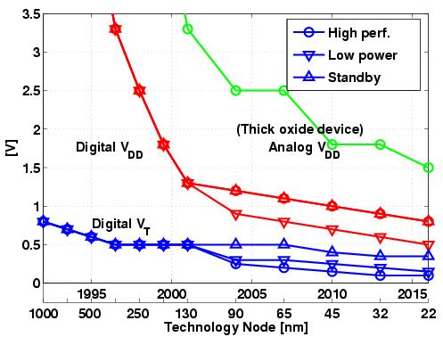
Figure 1: Supply and threshold voltage scaling over time as line widths decrease. [1]
In this work, a number of techniques are investigated to enable true low voltage operation without voltage boosting. These include the use of weakly inverted devices where feasible, the use of the body node as a fourth control or signaling terminal, and the use of circuit topologies avoiding stacked transistors. To explore the synergistic use of such techniques, we have designed two OTAs, an automatically-tuned 5th-order low-pass filter, and a track-and-hold circuit. The operation of these circuits have been pushed to supply voltages as low as the VT of the standard devices, in our case, 0.5V.
Forward biasing of the body-source junction has been applied in several low voltage digital circuits and in this work, it is applied to lower the VT of the devices. We typically apply a forward bias of 250mV which results in a lowering of the VT by about 50mV. There is little risk of latch-up in the context of 0.5V operation, since parasitic bipolar devices cannot be activated even when the full power supply is used as a forward bias.
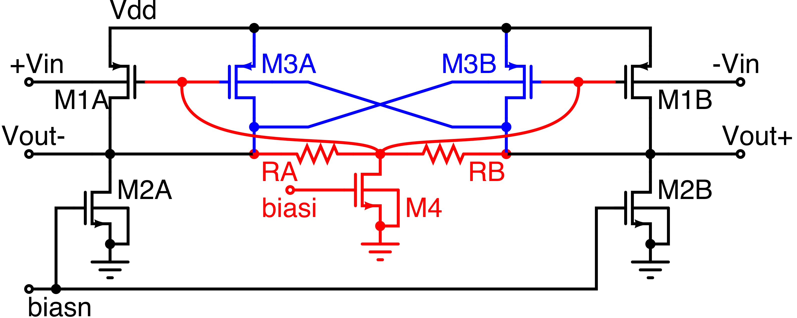
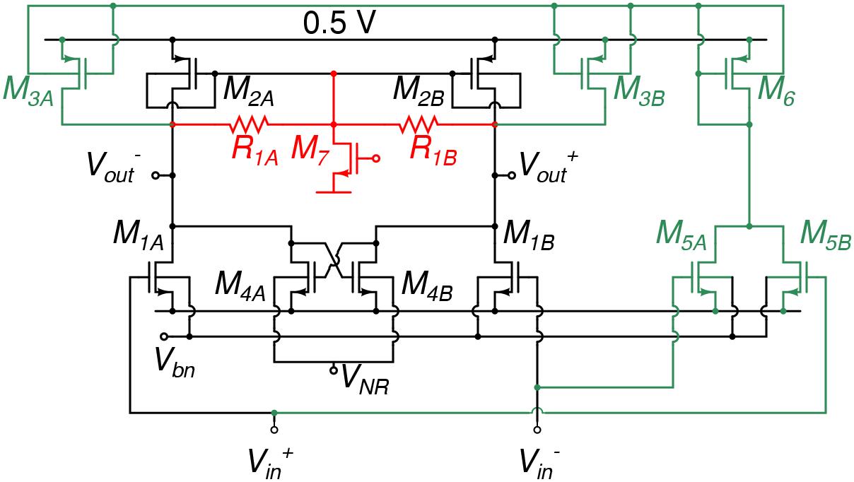
Two OTAs have been designed for operation at 0.5V. First, a body-input OTA, where the inputs are through the bodies of the devices whereas the biasing is through the gates. An input stage of this amplifier is shown in Fig. 2(a). In an alternate approach we have designed a gate-input OTA, where the inputs are through the gates of the devices and biasing is achieved through the bodies. An input stage of this amplifier is shown in Fig. 2(b). A detailed analysis of both of these circuits is in [2].
 |
 |
| (a) | (b) |
| Figure 2: Fully differential (a) body-input OTA stage, (b) gate-input OTA stage, with local common-mode feedback. | |
Both of these designs are for a 0.18µm CMOS process with standard devices of |VT| close to 0.5V. Robust biasing techniques that maintain circuit functionality and maximize swing over process, temperature and power supply voltage variations are developed. The body-input OTA has a measured DC gain of 52dB, bandwidth of 2.5MHz, and a power dissipation of 110µW for a 0.5V power supply. The gate-input OTA has a measured 62dB DC gain, 10MHz of bandwidth and a 75µW power dissipation for a 0.5V power supply.
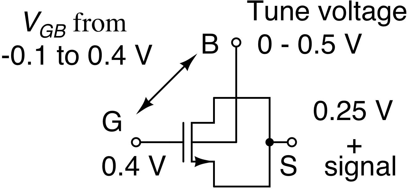
A tunable integrator is the basic building block of a tunable filter. We have investigated the use of varactor-R techniques. Variable capacitors, along with resistors and low voltage OTAs, enable us to build active-RC circuits at 0.5V. For this, we have proposed the use of a weak-inversion MOS capacitor as a three-terminal varactor.
 |
 |
| (a) | (b) |
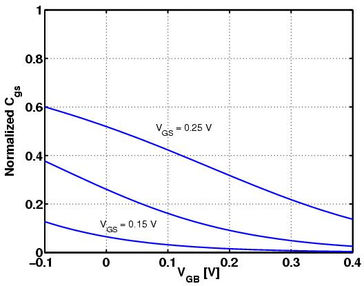
| Figure 3: (a) Gate (G) to Source/Drain (S) capacitance tuned by Body (B). (b) Normalized capacitance as a function of VGB for different VGS. Na= 3.5×1017cm-3, VFB=-1V. | |
The capacitance is between the gate and the combination of drain and source, denoted here as Cgs, and the tuning voltage is applied at the body, as shown in Fig. 3(a). In strong inversion and in accumulation, this capacitance is the oxide capacitance, Cox. In depletion, the intrinsic capacitance is zero as there is no inversion layer. From weak to strong inversion through moderate inversion, the intrinsic Cgs changes from zero to Cox. Changing the body voltage changes the device threshold voltage, VT, and also changes the inversion level of the device. This changes Cgs and the device now behaves as a three-terminal varactor.
The proposed varactor has been extensively analyzed, modeled and compared to measurements in [3].
To demonstrate the capabilities and synergy of the proposed ultra-low voltage design techniques, we designed a 5th-order low-pass elliptic filter with a 135kHz cut-off frequency. For minimum sensitivity requirements, a leap-frog topology was used. The capacitors are replaced with weak-inversion low-voltage MOS varactors. An ultra-low voltage voltage-controlled oscillator (VCO) was built using tunable integrators and resistors and capacitors matched to those in the filter. A phase-locked loop is built around the VCO using an XOR gate as a phase detector.
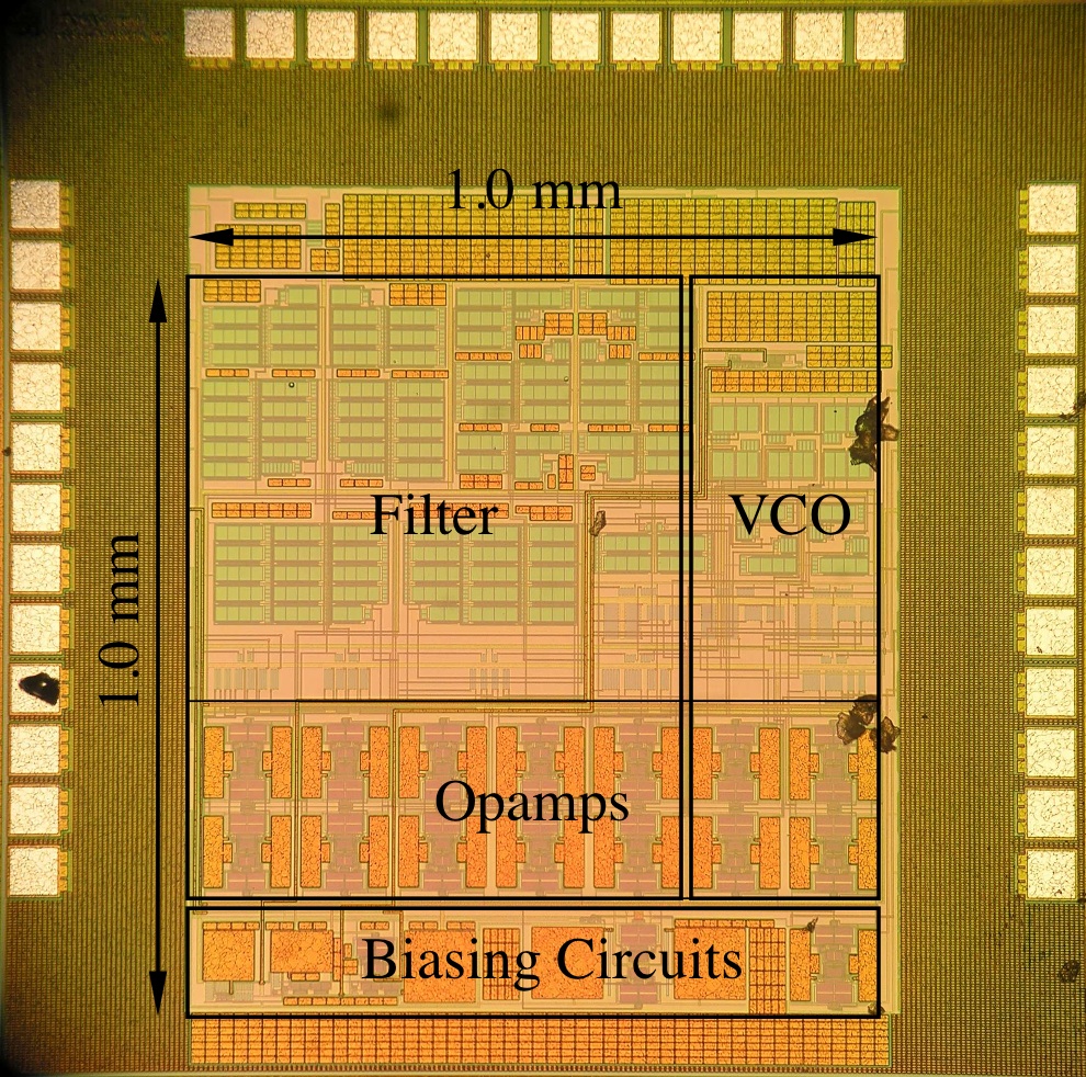
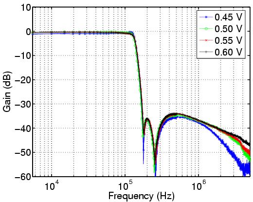
The chip including the 5th-order filter, VCO, bias circuits and phase detector was laid-out and fabricated on a 0.18µm CMOS process, taking advantage of triple well nMOS devices, high-resistivity resistors, and MIM capacitors. The total active chip area was 1mm×1mm. The chip micrograph is shown in Fig. 4(a). The filter was extensively characterized at different power-supply voltages, at different tuning voltages, and at different temperatures. The measured performance of the filter at different power supply voltages is shown in Fig. 4(b) and Table I. Nominally, a 57dB of dynamic range was observed for a power consumption of 1.1mW from a 0.5V power supply. The filter is operational in a temperature range from 5°C to 85°C.
 |
 |
| (a) | (b) |
| Figure 4: (a) Chip micrograph. (b) Measured filter characteristics at different power supply voltages. | |
| VDD [V] | 0.45 | 0.5 | 0.55 | 0.6 |
| -3dB cut-off frequency [kHz] | 135.0 | 135.0 | 135.0 | 135.0 |
| Total current [mA] | 1.5 | 2.2 | 3.3 | 4.3 |
| Noise¹ [µV rms] | 87 | 74 | 68 | 65 |
| Input² [mV rms] (20kHz / 1% THD) | 80 | 80 | 80 | 80 |
| Input² [mV rms] (100kHz / 1% THD) | 50 | 50 | 50 | 50 |
| In-band IIP3 [dBV] | -5 | -3 | -3 | -3 |
| Out-of-band IIP3 [dBV] | 3 | 5 | 3 | 5 |
| Dynamic range³ [dB] | 55.2 | 56.6 | 57.3 | 57.7 |
| Tuning range [kHz], Vtune = VDD | 96 | 88 | 84 | 69 |
| Tuning range [kHz], Vtune = 0.0V | 153 | 154 | 148 | 150 |
| PLL tone feed-thru [µV rms] @280kHz | 104 | 85 | 72 | 72 |
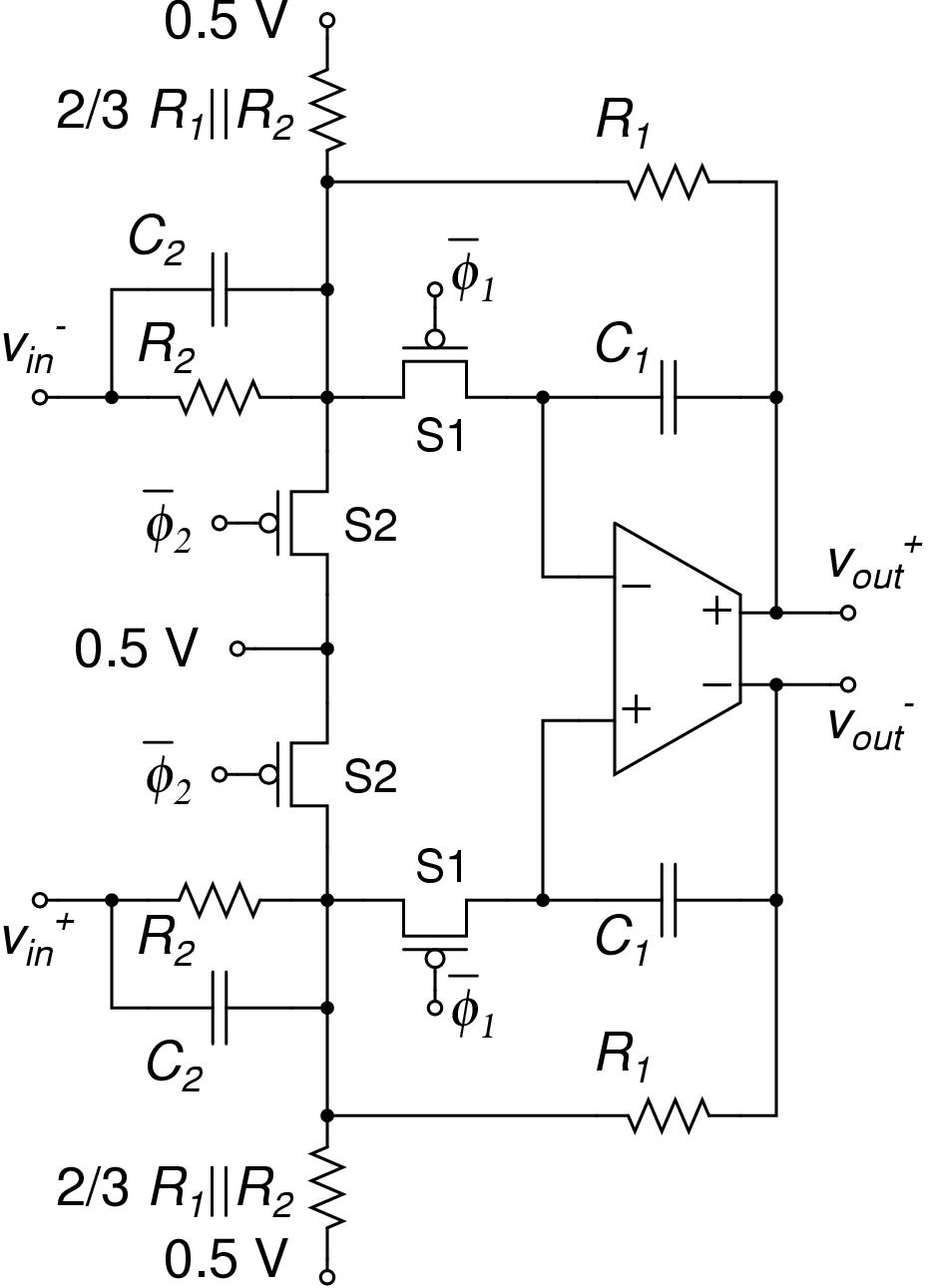
The ability to track and then sample an analog signal is often an essential function in signal acquisition interfaces. When a signal is sampled onto a capacitor using a transmission gate, the input voltage can swing from rail to rail only when the supply voltage is greater than the sum of the nMOS and pMOS VTs. In our work, an ultra-low voltage track-and-hold (T/H) circuit has been developed, that operates from a 0.5V power supply. The T/H circuit is configured in a way that the switches do not see full-swing signals. The switches are placed at the virtual ground associated with the input of an opamp in feedback configuration.
 |
 |
| (a) | (b) |
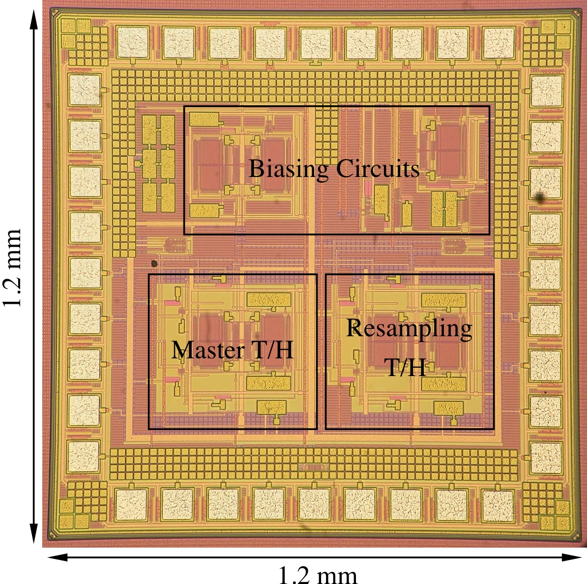
| Figure 5: (a) Fully differential 0.5V T/H circuit. φ1 and φ2 are non-overlapping clocks. (b) Chip micrograph. | |
Fig. 5(a) is the basic circuit used in a 0.5V fully-differential T/H circuit. Two cascaded T/H circuits were designed on a 0.25µm process. The pad-limited chip had a total area of 1.2mm×1.2mm and the die photograph is shown in Fig. 5(b).
This work has investigated design techniques for analog integrated circuits operating at a 0.5V power supply voltage. The work is motivated by the need to be able to design circuits for nano-scale devices which can tolerate only ultra-low voltages. The circuits presented are all true low-voltage circuits -- all nodes in the circuits are within the power supply rails of 0 and 0.5V. Standard devices in 0.18µm and 0.25µm technologies were used and these devices have a VT greater than or equal to the power supply voltage of 0.5V. This work thus demonstrates analog circuit design techniques at supplies lower than the device threshold voltages. It can be expected that with the advancement of nano-scale technologies, and the availability of lower threshold voltage devices, better performance will be attained.
Part of the work was supported by Analog Devices Inc. The T/H circuit was fabricated with the support of Philips Semiconductors. We would like to thank Tawfiq Musah, Ajay Balankutty, Edward Chiang and Junhua Shen for helping out in numerous experiments. Thanks to Profs Ken Shepard and Robert Melville for allowing the use of their equipment.
| [1] |
ITRS.
The International Technology Roadmap for Semiconductors
(2004 edition), 2004.
Technical Report, http://public.itrs.net. [ http ] |
| [2] |
S. Chatterjee, Y. Tsividis, and P. Kinget.
0.5-V analog circuit techniques and their application in OTA
and filter design.
IEEE Journal of Solid-State Circuits,
pages 2373-2387, Dec. 2005. [ http ] |
| [3] |
S. Chatterjee, T. Musah, Y. Tsividis, and P. Kinget.
Weak inversion MOS varactors for 0.5 V analog integrated filters.
In Symposium on VLSI Circuits, Digest of Technical Papers,
pages 272-275, Jun. 2005. [ http ] |