
If you haven't read the CAD tool information page, READ THAT FIRST.
In this handout, we are going to learn the following :
By now, you would have known how to enter and simulate your designs using Hspice. The next step in the process of making an integrated circuit chip is to create a layout. What is a layout? A layout is basically a drawing of the masks from which your design will be fabricated. Therefore, layout is just as critical as specifying the parameters of your devices because it determines whether yours is a working design or a flop!
There are 2 ways of doing a layout: manual and automated. Manual layout usually enables the designer to pack his devices in a smaller area compared to the automated process but it is more tedious. The automated process, on the other hand, is done using standard cells and usually takes more real estate space but it is much faster. In this tutorial, you will learn how to perform manual layouts and a simple inverter layout will be shown.
Before we get into the layout, first you need to understand the design rules for layout. The design rules which we will be using is the tsmc 0.25u Mixed signal CMOS Rules. Design rules give guidelines for generating layouts. They dictate spacings between wells, sizes of contacts, minimum spacing beween a poly and a metal and many other similar rules. Design rules are essential to any successful layout design, since they account for the various allowances that need to be given during actual fabrication and to account for the sizes and the steps involved in generating masks for the final layout. The design rules that we will be using can be read at : Note that the layout is very much process dependent , since every process has a certain fixed number of available masks for layout and fabrication. For the case of this tutorial, we are using a tsmc 0.25u CMOS process, which is a nwell process and supports one poly and five metal layers.
Before we proceed any further, please make sure that your present
library is associated with a techfile. For this , choose from the main cadence window
(also called CIW or command interface window) Technology File --> Attach to...
. A form appears on the window. On "Design Library", choose your working library and
on "Technology library" choose tsmc025 . Make sure that "cell" and "view" options
are NOT checked.
1. Create a layout cellview of the cell. Here we will create a
layout for the inverter cell.
In the library manager windown, click on the File
--> New --> CellView. Choose CellName as inverter and View
Name as layout. Then click on the OK button.
An empty Layout editor window will pop-up alongwith an LSW( called "Layer Selection Window") window.
The LSW window will show all the layers like nwell, pwell, active etc.
for the given process. An alternate way to open the layout editor
window, click on "Layout" in the View window
for inverter cell in the Library manager window. Then click on File
--> Open.
If the LSW window is blank, then there is an error.
The LSW window should look something like this:
If LSW looks different, then the most probable error is that your library is not attached to the Technology Library "tsmc025". You should attach you library to this technology file as described earlier on this page.
We are ready to draw objects in the layout window. Choose Create --> Instance
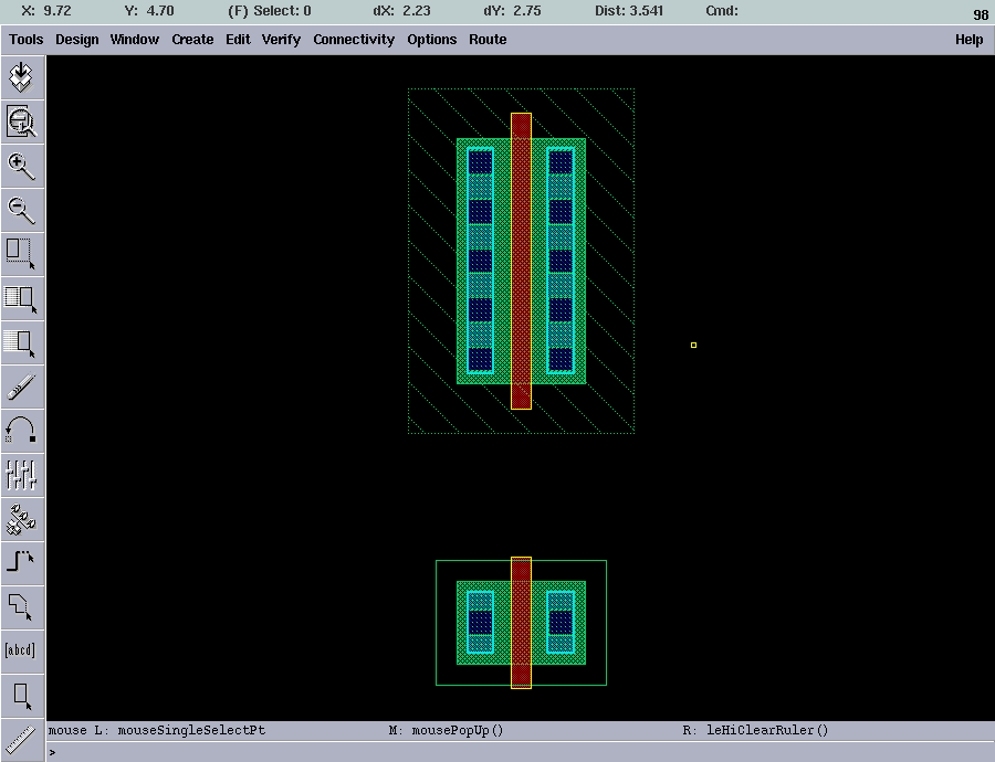
Choose "library" as tsmc025 and "cell" as pmos
"view" as layout , "width" as 3u . Everything else should be set by default.
Take a look at other parameters. You will see that "number of fingers" is 1 and
"length" is 240.00n (or 0.24u) which is by default the minimum possible channel length
for tsmc 0.25u technology. Shift-f and Ctrl-f will let you desplay and not display the layout
contents of the parametrized pmos transistor that you have just instantiated. Hitting Esc will
cancel the command and will stop the placing of repeated instances. Now, similarly place an nmos
with width 1u. Place it suitably below the pmos. At this stage, Your layout should look like as shown below :
Now that you have placed both transistors, you need to make connections between
them to create an inverter. We also need to place substrate and n-well contacts. Before drawing any wires, you
need to select the correct drawing layer from the layer selection window (LSW) .
First choose "metal1 dg" from LSW . By using create --> rectangle or create --> path.
Note that drawing paths is a little tricky. You will need to practice a little bit.
To end a path you have to double click with your left mouse button. Add in the wire connecting
the drains of both nmos and pmos which will serve as the output of the inverter. Do the same
for the poly connection between the gates. This time choose "ploy1 dg" from LSW. Note that
create --> path automatically chooses min. width for the path. To change this, you need to
hit F3 while the command is active and an option form will appear in which you can change the width.
By using create --> rectangle or create --> path , you can also make VDD and GND buses
(VDD on top of pmos and gnd on bottom of nmos). Also connect the source of pmos to this VDD bus and
that of nmos to GND bus. To place the substrate and n-well contacts, choose create --> contact .
From the menu, you can choose any type of contact . For substrate connection you need "m1_p" contact and
for n-well connection, you need "m1_n" contact. You also need "m1_poly" contact for connecting
metal1 to the poly gate of your inverter so that a signal on its input can come from outside
world on metal 1 and directly be applied to the gate of inverter.
After all this exercise, your layout should look like as below :
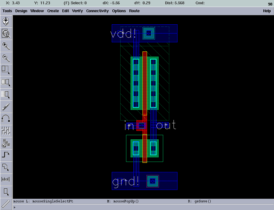
Note that above I have also placed pins by hitting ctrl-p. If you turn on the "display pin name" option, you can see those names as in above figure. And also I have extended n-well by drawing a rectangle of nwell abutting the existing n-well in order to cover the m1_n (n-well contact). With this we have completed the layout of an inverter. Some very important key points that might cause you trouble are listed below :