Mixer Design
Specifications
§ NF < 10dB
§ Voltage Conversion Gain > 8dB
§ Double Balanced Mixer
§ IIP3 > -5dBm
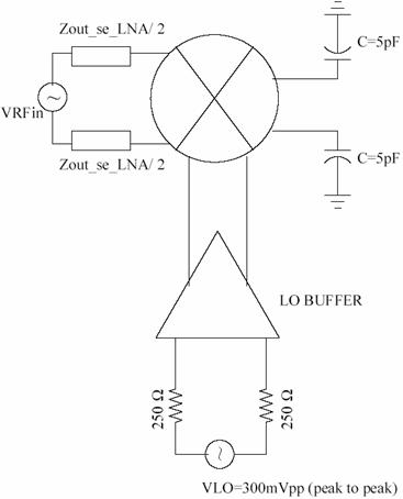
§ For LO=300mVpp and Power(RFIN)=-30dBm
LO leakage at RFIN < -25dBm
LO leakage at IFOUT < -20dBm
Please assume 1% mismatch at each differential pair.
Input and Output Interfaces: The impedance of the source that drives the mixer is the impedance seen from your LNA output. Please measure the output impedance of your LNA and model it as the impedance of the signal source driving your mixer at the frequency range of interest. The single ended output load of your mixer is a capacitor of 5 pF.
Simulations: The specifications given above are for ‘tt’ (typical, typical process) and 25°. You also have to simulate your design at ‘ss’ and ‘ff’ corners, and -40° and +85° temperatures.
Submission: You have to submit the following materials on November 3rd, 2004
§ Transistor level schematic of your design
§ Top-level schematics for all test setups. (Before you submit your design, please create a symbol for your LNA and bring out all input, output, power supply and bias pins. Then create top-level test benches, and submit them with your design. You don’t have to submit the same schematic again and again since you are simulating for different corners or different temperature.)
§ Simulation results at all temperatures and corners. Please make a table of the results for different corners and temperatures.
Please submit all your works in one pdf or postscript file. You don’t need to make any hardcopy submission, unless you have to or want to show any calculations. If you are working in groups, please cc with the e-mail and the name of your partner.
Links
§ http://www.maxim-ic.com/quick_view2.cfm/qv_pk/1919/ln/