LNA + Mixer Design Specifications
Note: Originally we should have two or more gain settings for the LNA. The high gain is required to amplify the small signals and reduce the noise figure constraints of the stages following LNA (Please check the noise figure calculations of cascaded blocks in Razavi’s RF Microelectronics book). However, the high gain of LNA is not necessary for large signals. Indeed, for very strong signals high gain of the LNA will introduce third order harmonics inside the band. Thus, a common practice in front-end designs is to use multi gain settings for the LNA: high gain for the weak signals and small gain for the strong signals. However, in this project we just asked you to design LNA for one gain setting. Thus, for this assignment and the final submission we are going to make a difference in measuring NF and distortion.
§ NF < 12.5dB
Assume that we have the high gain setting for the LNA (which is the gain you have designed for during the first assignment.).
§ Distortion: Includes two tests as it is explained in the specs.
1) Inband IM3 : Two (-10-LNA_gain) dBm inband sinusoid signals (i.e 2410 MHz and 2414 MHz) should not create IM3 products higher than (-20-LNA_gain) dBm.
Note: For this test, we assume that LNA
has 0dB gain, since the desired signal is strong. For example, if your LNA gain
is 15dB, then you should feed two -25dBm sinusoid signals to the input of your
system, and the IM3 products inside the band should not be higher than -35dBm.
2) Outband IM3: When desired signal level is -70 dBm, two -35 dBm adjacent channel blockers (i.e 2437 MHz and 2467 MHz sinusoid signals) should not create input referred IM3 products higher than -80 dBm.
Note: For this test we assume high LNA gain setting, since the desired signal level is low.
§ Input Return Loss < -15 dB @ 2450 MHz
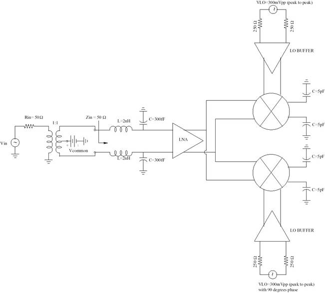
Input and Output Interfaces:
Simulations: The specifications given above are for ‘tt’ (typical, typical process) and 25°. Due
to the time constraints, it is sufficient to simulate your design at ‘tt’ and 25° just for this assignment.
Submission: You have to submit the following materials on November 3rd, 2004
§ Transistor level schematic of your design
§ Top-level schematics for all test setups. (Before you submit your design, please create a symbol for your LNA, Mixer and LO buffer, and bring out all input, output, power supply and bias pins. Then create top-level test benches, and submit them with your design.)
§ Please make a table of the results.
Please submit all your works in one pdf or postscript file. You don’t need to make any hardcopy submission, unless you have to or want to show any calculations. If you are working in groups, please cc with the e-mail and the name of your partner.