Final Design Specifications & Project Report
Note: This assignment includes the final project report and the following simulations (similar simulations that you have done for assignment #3) of the whole system
Simulations: The following specifications are given for ‘tt’ (typical, typical process) and 25°. You also have to simulate your design at ‘ss’ and ‘ff’ corners, and 0°
and +85° temperatures.
§ NF < 12.5dB
Assume that we have the high gain setting for the LNA (which is the gain you have designed for during the first assignment.).
§ Distortion: Includes two tests as it is explained in the specs.
1) Inband IM3 : Two (-10-LNA_gain) dBm inband sinusoid signals (i.e 2410 MHz and 2414 MHz) should not create IM3 products higher than (-20-LNA_gain) dBm.
Note: For this test, we assume that LNA
has 0dB gain, since the desired signal is strong. For example, if your LNA gain
is 15dB, then you should feed two -25dBm sinusoid signals to the input of your
system, and the IM3 products inside the band should not be higher than -35dBm.
2) Outband IM3: When desired signal level is -70 dBm, two -35 dBm adjacent channel blockers (i.e 2437 MHz and 2467 MHz sinusoid signals) should not create input referred IM3 products higher than -80 dBm.
Note: For this test we assume high LNA gain setting, since the desired signal level is low.
§ Input Return Loss < -15 dB @ 2450 MHz
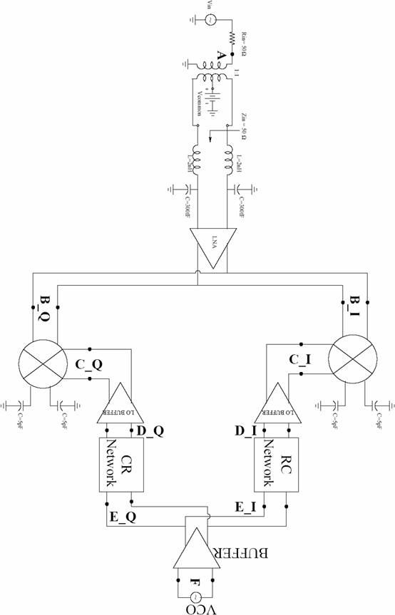
§ Run a transient simulation with RFin at 2.412 GHz and VCO frequency at 2.4 GHz, and show the signals at the each point shown in the following figure.
Input and Output Interfaces:
Final Submission & Project Report: You have to submit the following materials on December 15th, 2004.
§
Simulation results of the final assignment.
Please make a table of the results. (Similar submission style as it is for
the previous assignments. But you don’t need to submit any circuit schematics.)
Note: This is separate from the final
project report.
§ You should hand in a brief Journal of Solid State Circuits style report. The length of the report should not exceed six pages(not including figures/tables). It should contain all circuit schematics, simulation plots that you want the professor/grader to see. The figures and the tables should be at the end of the report, and large enough so everything is well readable. ( LaTeX style files, Microsoft Word author's template.)
Important: 1) You need to make a spreadsheet of your receiver design; noise figure and linearity calculation.
2) You need to make a level diagram of the receiver as the example Dr. Kinget distributed in the class.
3) Please make a table of simulations results for each block (LNA, Mixer, VOC and Quadrature) that you are presenting. Include the minimum, typical and maximum values for each specification as it is done in a typical datasheet.
4) Also summarize the performance of the overall design in a datasheet. Consider the datasheet of MAXIM product as an example.
NOTE: Final project report is due to
December 15th, 2004 at 2:00pm sharp. You can submit the simulation
results of the final assignment and zip file of your design library later on
the same day. But you have to submit the project report before 2:00pm.
§ You should tar/gzip your design library so that in case we need to check, we can rerun the required simulations. Have a file called "README" inside the tar/gzip of your database which essentially describes what is what and gives pointers to how to do important simulations.
Please submit all your works in one pdf or postscript file. You don’t need to make any hardcopy submission, unless you have to or want to show any calculations. If you are working in groups, please cc with the e-mail and the name of your partner.