EECS 4340: Computer Hardware Design
TOOLS TUTORIAL: FPGA Synthesis and Place-and-Route
Important Note:
This tools flow applies only to those doing the PDP-8 using both XC4010E FPGA parts. The DDR S-DRAM controller uses more advanced Xilinx parts and requires a different design flow. The tools for the flow described below are only available on the Sun workstations; they are not available under Linux.
We will be using two XC4010E FPGA parts for our PDP-8. One will be used to hold the datapath and the other will be used to hold the controls. In our flow, we will be using the Sun workstations for synthesis and mapping to the FPGA. We will then transfer the "bit stream" (.bit) file for the slave serial programming of the FPGA over to the PCs in Mudd 1211. The Impact program on the PCs will be used to download the FPGAs through the Multilinx cables.
To test out the design flow, you will walk through a simple design, such as the library light in the directory
/tools2/courses/ee4340/cdslib/light
or you can work with the datapath of your PDP-8 directly.
STEPS
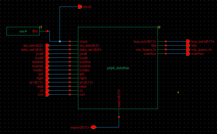
1. You will need to make a few modifications to the design to handle the clocks. Before you start it is a good idea to make a back-up copy of your previous datapath. We will be using a 8 MHz local oscillator on the "datapath" FPGA and this clock will be used for the logic in both FPGAs. To do this, you will need to create a component in your datapath schematic called osc4 with a single output (no inputs) called f8m . This output should be connected to the clock of your datapath design. To feed the clock into your controller you will need to make a corresponding output pin on the datapath. Your controller schematic should now consist of the controller block and the uart_interface, there should be no SRAM in either the datapath or the controller schematic.
2. To synthesize your VHDL with Synopsys FPGA Compiler II, bring up the VHDL toolbox from Cadence by choosing Tools > VHDL Toolbox. Then from the VHDL Toolbox, choose Commands > Synthesis. Your design will be "checked-and-saved" again and the Cadence-To-Synopsys (CSI) form will appear.
3. From this form, choose the option to create a command file called "netlist.inc." We will refer to this file to find the paths to all the VHDL files and the order in which these files have to be analyzed by the synthesis tool. Unfortunately, the syntax used is that for the Synopsys Design Compiler, and Synopsys (in their infinite wisdom) decided to use a different syntax for FPGA Compiler II. Change all the "analyze -work pdp8 -f vhdl" to "add_file -library pdp8 -format vhdl" Also make sure you remove the "/../computer_name/" from the path of each file.
4. Copy the template command file into your run directory. You will find this template file in
/tools2/courses/ee4340/public/xc4010.cmd
You will need to modify this file. Copy the paths from the "netlist.inc" file. Your *.cmd file should look like this:
create_project pdp8_dataflow_syn_proj create_library pdp8 vhdl.vhd add_file -library pdp8 -format VHDL /path . . . . add_file -library pdp8 -format VHDL /path analyze_file -progress create_chip -library pdp8 -progress -name pdp8_dataflow_syn -target XC4000E -device
4010EPC84 -fast -speed -3 -frequency 8 -preserve pdp8_dataflow_syn
current_chip pdp8_dataflow_syn optimize_chip -name pdp8_dataflow_syn-optimized -progress report_timing export_chip -dir (name of directory to export design to) list_message
Please change the above file accordingly for the controller.
5. To execute this command file type
fc2_shell < xc4010.cmd > fc2.out &
This will run FPGA Compiler II, storing the results in the log file. If this is not your first time running this command file you will need to remove the directory with the command "rm -rf proj_name" You must carefully scrutinize the log for error and warning messages which may indicate problems in your design. Please see me if you have an error that you do not understand. The other very important thing you need to scrutinize are the tables of "inferred memory" devices that come from synthesizing your VHDL process statements. You must make sure that FPGA Compiler II creates the latches you expect only for the process statements for which you intended to create latches. You should not have latches from process statements representing combination logic (for example, for the combinational logic of FSMs). In you do, it means that you have broken one of the rules (e.g., haven't put all the inputs into the process' sensitivity list, haven't covered all cases with a "default" section at the top of the process).
6. Now you will need to copy the *.pcf (pin constraints) file for both the datapath and controller from the directory
/tools2/courses/ee4340/public/dataflow.pcf or controller_uart.pcf
for the dataflow and controller respectively.
7. Once the files are copied over you want to concatenate your *.pcf with your *.ncf file. The *.ncf file will be generated when you run the fc2_shell. Use this command
>cat *.pcf *.ncf > *.ncf.
This will combine your timing and pin constraints. Then you will need to go into the *.ncf file and for the controller file comment out all the timing constraints except for the clock timing. For the datapath *.ncf file comment out everything including the clock timing.
The basic clock frequency of the design is specified in the create_chip command found in your *.cmd file. We have specified a 8-MHz clock. We have a simple flop-based design, in which the clock cycle time (125 nsec) constrains most of the paths. To constrain paths from the primary inputs and outputs, you would in general need to specify arrival times on inputs or required arrival times on outputs. For the time being, we will not consider how to add these, but it may become necessary later to do this. These timing constraints (as well as the clock constraints) are exported to a constraint file with the *.ncf extension. The netlist for the design is found in the *.edf file; this file is in EDIF (Electronic Design Interchange Format). Both the *.edf and *.ncf files will be imported into the Xilinx ISE tool.8. To place and route the designs, bring up the Xilinx ISE tool by typing ise& at the UNIX command prompt to bring up the ISE GUI. Choose File > New Project. For Project Location, use the run directory you have been working in. Choose an appropriate project name. Select the Device Family of XC4000E. The Device is xc4010e-3pc84. The Design Flow is EDIF. Now choose Project > Add Source Attach both the *.edf and *.ncf files to the project. Now in the "Processes For Current Source" window, select "Implement Design." With the right mouse button, select "Run." This will run technology mapping and place-and-route your FPGA design. If this completes without errors, select "Generate Programming File." With the right mouse button, select "Run" which will generate the bit file for download to the FPGAs. This file will have the *.bit extension in your run directory. You may also wish to invoke the timing analyzer to check the timing of your design. Please work with me or the TA to understand how to do this.
9. Now, you will have to copy the bit stream files over to the PC's in Mudd 1211.