|
|
Spring 2014 Seminars
|
|
Title : Compact Thermal Sensors in Intel Processors from 90nm to 22nm
Speaker: Dr. Joseph Shor,
Intel Yakum
Date: Monday, Deb 17th, 12:00pm-1:00pm, 825 Mudd
Title : A simple method to calculate the power spectrum of distorted wide-band signals
Speaker: Dr. Alessandro Piovaccari,
Silicon Labs
Date: Friday, March 14th, 2:00pm-3:00pm, 227 Mudd
Title : Cognitive Radio Transceiver Chips (SSCS Distinguished Lecture)
Speaker: Dr. E.A.M.Klumperink,
University of Twente
Date: Monday, March 31st, 12:00pm-1:00pm, 825 Mudd
Title : Challenges of Calibrated Time-Interleaved High-Speed ADCs
Speaker: Dr. Aaron Buchwald,
Entropic Communications
Date: Friday, April 4th, 2:00pm-3:00pm, 227 Mudd
Title : Microelectronic Test Structures for CMOS Technology
Speaker: Dr. Mark B. Ketchen,
OcteVue
Date: Thursday, April 10th, 2:00pm-3:00pm, 414 CEPSR Mudd
Title : VLSI Architectures for Communications and Signal Processing
Speaker: Dr. Kiran Gunnam,
Violin Memory
Date: Friday, May 2nd, 2:30pm-4:30pm, 750 Interschool Lab, CEPSR
Title : A 48-mW 18-Gb/s Fully Integrated CMOS Optical Receiver with Photodetector and Adaptive Equalizer
Speaker: Prof. C. Patrick Yue,
HKUST
Date: Friday, May 30th, 11:00am-12:00pm, 825, MUDD
Title : Beyond 60GHz - CMOS Circuits and Techniques for More Bandwidth, Power and Efficiency
Speaker: Dr. Eran Socher,
Tel Aviv University
Date: Friday, May 30th, 2:00pm-3:00pm, 414, CEPSR
|
|
|
|
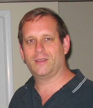
Dr. Joseph Shor,
Intel Yakum
Date:
Monday, Feb 17th, 12:00pm-1:00pm
Location:
825 Mudd
|
Compact Thermal Sensors in Intel Processors from 90nm to 22nm
Abstract:
Temperature sensing and regulation in microprocessors are important for power management and have a direct influence on power/performance. When the chip gets too hot, its frequency gets lowered in a process called throttling, in order to prevent it from exceeding the maximum reliable operating point. As temperature is lowered, the frequency of the chip can degrade because of the ITD effect (Inverse Temperature Dependence). In this case, information from the thermal sensor is used to raise the supply voltage to maintain performance. The thermal sensor is also used for fan regulation and prevents the chip from burning itself up in thermal runaway. In the older chips, there was a single core, so it was sufficient to have one or two thermal sensors per IC, and the power and area were not very important. Since the industry shifted to multicore, there can be as many as 25 sensors per chip, so their area and power have become substantial. In addition, analog circuits tend to have very poor scaling between process generations, or even reverse scale. In the Nehalem generation the thermal sensors occupied more than 1% of the overall die area, and consumed > 200mW, so there was much motivation to scale them down.
In our group in Yakum, Israel, we have developed compact and power-efficient thermal sensors. Using novel analog architectures and circuit techniques the area and power were scaled by > 10X in the same process generation. The level of scaling in analog is virtually unheard of. In the Sandy-Bridge processor, we implemented an NMOS based sensor, which measured the temperature dependence of threshold voltage (Vt) and mobility (Mu) and output a temperature-dependent frequency.
In addition, we also developed a very compact diode-based thermal sensor which used a band-gap reference to generate a temperature-dependent voltage, which was measured using a frequency-based analog-to-digital converter. The diode sensor is considered more reliable than the NMOS based design since Vt and Mu change during the process evolution. The 22nm sensor was one of the world's first analog circuits reported at this process node.
These sensors have been benchmarked as the smallest IC thermal sensors in the art, with sizes < 0.006 mm2. They also have a very fast sampling speed (> 5kS/sec), which enable them to capture fast thermal transients on the processor. The designs are very robust and can be manufactured with > 99.9% yield.
The evolution of these sensors from 90nm down to 22nm will be discussed, along with some of challenges inherent in designing analog circuits in the noisy, pure-digital environment of a microprocessor.
Biography:
PhD in Electrical Engineering from Columbia University, 1993. BA in Physics, Queens College, 1986.
Shor has published more than 50 papers in refereed Journals and Conference Proceedings in the areas of Analog Circuit Design and Device Physics. He holds 35 issued patents and several pending patents. Since 2004, he has been at Intel Corporation, where he is presently a Principal Engineer, and head of the Analog Team at Intel Yakum in Israel. Between 1999-2004, he worked at Saifun Semiconductor as a Staff Engineer where he established the analog activities for Flash and EEPROM NROM memories. From 1994-1999, he was a Senior Analog Designer at Motorola Semiconductor in the DSP Division. From 1988-1994, he was a Senior Research Scientist at Kulite Semiconductor, where he developed processes and devices for Silicon Carbide and Diamond Microsensors. His present interests include Switching and Linear Voltage Regulators, thermal Sensors, reference circuits, PLLs , IO circuits, and low voltage/power analog circuits. He is also interested in microsensor design, physics and applications. He is an IEEE Senior Member and a member of the ISSCC Technical Program committee.
|
|
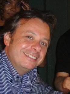
Dr. Alessandro Piovaccari,
Silicon Labs
Date:
Friday, March 14th, 2:00pm-3:00pm
Location:
227 Mudd
|
A simple method to calculate the power spectrum of distorted wide-band signals
Abstract:
The correct analysis of distortion products is one of the most important aspects in the design of low-power low-cost communication devices. There is a fundamental trade off between cost, power and dynamic range of the system. More precisely, the lower and upper boundaries of the dynamic range are determined respectively by the linearity and noise performance of the system, which in turn are determined by the technology choice, architecture and power consumption of the system itself. As an application example, a typical RF signal receiver is composed by a cascade of blocks performing operation of filtering, amplifying, frequency translation and data conversion. An almost century-long of literature on this topic has shown that for a given performance specification, the optimal design in terms of power consumption and cost is determined by a correct distribution of gain, filtering, and noise and distortion performance among the various blocks constituting the receiving chain. Another very important application is the determination of spurious spectral emission of a transmission system. Spectrum scarcity and pollution due to older standard (like the TV system) has forced government controlled agencies (FCC, ETSI, …) to define transmission regulations, including strict spectrum emission masks. This fact ultimately results on the architectural choice of the power amplifier of the transmitter, and the consequent trade-off between its linearity and power efficiency. As of today, the determination of the distortion products in weakly non-linear systems has been mainly relying on simplified sinusoidal analysis. While this analysis has the advantage of being simple enough to be usable in hand calculation or in spreadsheets, it produces good predictions results only for narrowband signals containing a strong carrier (FM, AM, …), but it is inadequate to predict the distortion effect on wide-band signals that have statistics similar to band-pass noise, like OFDM signals used in digital television (DTV) and Wireless Local Access Networks (WLAN). Several analysis has been performed in literature during the last 50 years to overcome the limitation of simple sinusoidal distortion analysis, but the math involved is generally quite complex and because of the wide availability of CAD and computation tools, system designers generally prefer to rely on time-domain simulations. This work, present a method to calculate the exact effect of distortion on wide-band signal signal that have Gaussian-like characteristics, including the determination of the exact power of the distortion products, and the prediction of effects like spectral corruption and spectral regrowth, that are not predictable by traditional sinusoidal analysis. It is important to note that, even if this method is based on results of advanced mathematics (Hermite polynomials), its results are simple enough to be usable in hand calculations, similar to sinusoidal distortion analysis. Moreover, the method can be use to calculate the exact power spectrum of the output of a non-linear system when a band-pass signal of non-negligible bandwidth and approximated by a Gaussian wide-sense stationary (WSS) random process is applied to its input, using simple matrix mathematics and without the need of a time-domain simulation.
Biography:
Dr. Alessandro Piovaccari received the Laurea and Ph.D. degrees in electronic engineering from the University of Bologna, Bologna, Italy, in 1993 and 1998, respectively and a Post-Master's Advanced Certificate with Honors in electrical engineering from Johns-Hopkins University, Baltimore, MD, in 2002. In 1997, he joined Tanner Research in Pasadena, CA as a Research Scientist in where he worked on the development of a CMOS image sensors with embedded motion detection. From 1998 to 2003 he has been part of the design services team as of Cadence Design Systems in Columbia, MD where he worked on CMOS RFICs for wireless communications and in Cary, NC where he managed the high-speed SerDes development. Since 2003, he has been part of Silicon Laboratories in Austin, TX where he contributed to the architecture definition and IC design of the single-chip FM radio, which as today sold more than 1.2 billion devices. He also managed the development and co-architected the single-chip TV tuner, currently employed in more that 55% of the TV sold world-wide. He currently holds a VP of Engineering position and he's responsible for the development of the MCU, wireless, and audio/video broadcast products. He's the author of 9 papers and 31 patents (20 currently issued). Dr. Piovaccari is a Senior Member of IEEE and Full Member of AES. He is part of the Technical Program Committee of CICC, where he also served as chair of the Analog Subcommittee. He has been reviewer for IEEE conference and journal including CICC, ISCAS, JSSC, MTT and CAS.
|
|

Dr. E.A.M.Klumperink
Univ. of Twente
Date:
Monday, March 31st, 12:00pm-1:00pm
Location:
Room 825, Mudd
|
Cognitive Radio Transceiver Chips (SSCS Distinguished Lecture)
Abstract:
A Cognitive Radio transceiver senses its radio environment and adaptively utilizes free parts of the radio spectrum. CMOS IC-technology is the mainstream technology to implement smart signal processing and for reasons of cost and size it is attractive to also integrate the radio frequency (RF) hardware in CMOS. This lecture discusses radio transceiver ICs designed for cognitive radio applications, with focus on analog RF. Cognitive radio asks for new functionality, e.g. spectrum sensing and more agility in the radio transmitter and flexibility in the receiver. Moreover, the technical requirements on the building blocks are more challenging than for traditional single standard applications, e.g. in bandwidth, programmability, sensing sensitivity, blocker tolerance, linearity and spurious emissions. Circuit ideas that address these challenges will be discussed, and examples of chips and their achieved performance will be given.
Biography:
Eric Klumperink received his PhD from Twente University in Enschede, The Netherlands, in 1997. He is currently an Associate Professor at the same university where he teaches Analog and RF CMOS IC Design and guides research projects focusing on Cognitive Radio, Software Defined Radio and Beamforming. Eric served as Associate Editor for TCAS-I and II, and for the Journal of Solid-State Circuits. He is a technical program committee member of ISSCC and RFIC and is Respected Lecturer for IEEE. He holds several patents, authored and co-authored more than 150 international refereed journal and conference papers, and is a co-recipient of the ISSCC 2002 and the ISSCC 2009 "Van Vessem Outstanding Paper Award".
|
|

Dr. Aaron Buchwald
Entropic Communications
Date:
Friday, April 4th, 2:00pm-3:00pm
Location:
Room 227, MUDD
|
Challenges of Calibrated Time-Interleaved High-Speed ADCs
Abstract:
The dream of moving the ADC of a communication receiver all the way to the antenna is fast becoming a reality. Recent ADCs that take advantage of time-interleaving and rely heavily on calibration enable new receiver architectures where the entire spectrum is digitized while all channelization and demodulation is done in the digital domain. Such systems that are "RF-to-Digital" have many advantages. However, the design of the requisite ADC remains a challenge to achieve wide-bandwidth and high dynamic-range at very low power. This talk introduces key concepts of calibrated time-interleaved ADCs at a tutorial level. Examples of specific solutions are presented. Advanced concepts are also introduced. Finally, students wishing to pursue this area as a research topic will be exposed to several unsolved issues and hopefully will be inspired to extend the state-of-the-art with new and creative solutions.
Biography:
Dr. Aaron Buchwald has 31 years of experience in the field of analog integrated circuit design. He is currently a Fellow at Entropic Communications after their recent acquisition of Mobius Semiconductor, where he was CEO and founder. Prior to founding Mobius Semiconductor, Dr. Buchwald worked at Broadcom, joining as one of the first members of the analog group with the charter to help build a world-class analog team emphasizing design in a mixed-signal environment.
Dr. Buchwald's work on embedded CMOS Analog-to-Digital Converters (ADCs) enabled the production of single-chip cable set-top boxes and cable modems with integrated analog front ends and DSP circuitry. His work was awarded the best paper prize in 1997 at ISSCC. Later, Dr. Buchwald was responsible for development of high-speed serial transceivers (XAUI, CX4 and Fiber Channel) at Broadcom. The initial XAUI transceivers were some of the first to employ adaptive receive equalization.
Dr. Buchwald was formerly an Assistant Professor at the Hong Kong University of Science and Technology (HKUST). In his early career, Dr. Buchwald spent two years as an analog IC designer at Siemens in Munich Germany. Prior to that, he was with Hughes Aircraft Company in El Segundo, CA.
Dr. Aaron Buchwald was born in Ames, Iowa and received a BSEE from the University of Iowa, Iowa City, Iowa, and an M.S. and Ph.D. from the University of California, Los Angeles. He is co-author of the book Integrated Fiber-Optic Receivers. He has taught professional short-courses on data converters and serial transceivers.
|
|
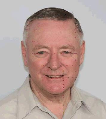
Dr. Mark B. Ketchen
OcteVue
Date:
Thursday, April 10th, 2:00pm-3:00pm
Location:
Room 414, CEPSR
|
Microelectronic Test Structures for CMOS Technology
Abstract:
In scientific investigation and in launching a manufacturing technology through its stages of research and development, test structures are used to facilitate characterization and control of key aspects of the integrated whole. With scaling to deep sub-um dimensions, the cost and complexity of CMOS technologies continues to rise. Appropriately designed test structures add efficiency and reduce cost and time to market. Examples of innovative CMOS test structures and measurement techniques covering from DC to multi-GHz frequencies are described. Emphasis is placed on a methodology that bridges both upward in the hierarchy to complex circuitry and downward to the properties of the constituent components. The designs and concepts presented are based on the work originally done for IBM's microprocessor chip technologies[1].
[1] Manjul Bhushan and Mark B Ketchen, Microelectronic Test Structures for CMOS Technology, http://www.springer.com/engineering/electronics/book/978-1-4419-9376-2
Biography:
Mark B. Ketchen is the sole proprietor of OcteVue, providing technical consulting services in microelectronic technologies. He earned his BS in Physics from MIT in 1970 followed by four years as a Naval Officer and completion of a Ph.D in Physics from UC Berkeley in 1977. He spent 36 years at IBM, holding a variety of positions in science and technology, ranging from individual investigator to serving as Director of IBM's international program in Physical Sciences. He was a pioneer in the design, fabrication and characterization of integrated dc SQUIDs, led design and test efforts in IBM's early attempt to build a superconducting computer, and has recently driven advances in qubits for quantum computing. He worked in silicon bipolar technology integration, ran the silicon fab line at IBM Research in the late 1980s, and worked on design and utilization of custom DC and high speed test structures for CMOS characterization and evaluation at the 180 nm through 32 nm technology nodes.
Dr. Ketchen has 43 issued or pending patents over 180 publications and is co-author of the book Microelectronic Test Structures for CMOS Technology published by Springer. He is a Life Fellow of the IEEE, a Life Fellow of the American Physical Society and a past recipient of the American Institute of Physics Prize for Industrial Applications of Physics and the IEEE Leeds award. He is a citizen of the US and Canada and holds a US Government security clearance.
|
|
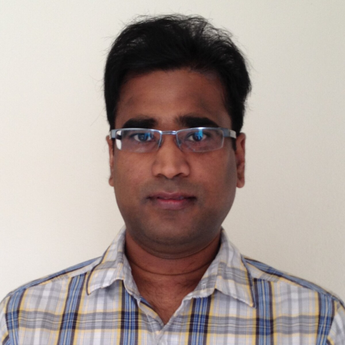
Dr. Kiran Gunnam
Violin Memory
Date:
Friday, May 2nd, 2:30pm-4:30pm
Location:
750 Interschool Lab, CEPSR
|
VLSI Architectures for Communications and Signal Processing
Abstract:
Part 1 of this lecture covers introduction to VLSI architectures for Communications and Signal Processing Systems. Various topics include pipelining and parallel processing, retiming, unfolding, folding, systolic architecture design and algorithmic transformations. The emphasis is how to design high-speed, low-area, and low-power VLSI systems for a broad range of DSP and communication applications.
Part 2 of this lecture covers speaker's research. Low-Density Parity-Check codes now have been firmly established as coding technique for communication and storage channels. This talk gives an overview of the speaker's research and contributions in the development of low complexity iterative LDPC solutions for Turbo Equalization for magnetic recording storage channels. Complexity is reduced by developing new or modified algorithms and new hardware architectures viz. system level hardware architecture, statistical buffer management and queuing, local-global interleaver, LDPC decoder and error floor mitigation schemes.
Biography:
Kiran Gunnam received the MSEE and PhD in Computer Engineering from Texas A&M University, College Station, TX. He currently works as Director of Engineering at Violin Memory. He previously held research and development positions at Nvidia, Certicom, LSI, Marvell Semiconductor, Starvision Technologies, Schlumberger, Intel and Texas Engineering Experiment Station.
Dr. Gunnam has extensive research and development work experience in complex data path and control path systems. Dr. Gunnam is an expert in IC implementation of communications and signal processing systems. His PhD research contributed several key innovations in advanced error correction systems based on low-density parity- check codes (LDPC) and led to several industry designs. He has done extensive work on ASIC hardware architecture, micro-architecture and digital IC implementation for different systems (IEEE 802.11n Wi-Fi, IEEE 802.16e WiMax, IEEE 802.3 10-GB, Holographic read channel, HDD read channel and Flash read channel).
Dr. Gunnam has around 75 patents/patent applications/invention disclosures on hardware architecture and micro-architecture (46 issued patents, 4 pending patent applications and 25 more invention disclosures). He is the lead inventor/sole inventor for 90% of them. He is an IEEE Senior Member. He is also an IEEE Solid State Circuits Society Distinguished Lecturer for 2013 and 2014.
|
|
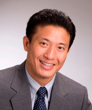
Prof. Patrick Yue
HKUST
Date:
Friday, May 30th, 11:00am-12:00pm
Location:
825, MUDD
|
A 48-mW 18-Gb/s Fully Integrated CMOS Optical Receiver with Photodetector and Adaptive Equalizer
Abstract:
The rising demand for short-range optical links using 850-nm wavelength has generated strong interest in CMOS optoelectronic integrated circuits (OEICs). Compared to existing hybrid solutions employing off-chip GaAs-based avalanche photodetectors (PDs), single-chip OEICs with on-chip PDs can lower optical module assembly cost and eliminate the parasitic effects due to the bond-wire and ESD protection circuit at the receiver input. However, CMOS PDs have poor responsivity (<50 mA/W) under standard supply bias due to their shallow junction depth (~1um) relative to the 850-nm light absorption length in silicon (>15um). Moreover, typical CMOS PD bandwidth (BW) is <100 MHz limited by substantial junction capacitance and large carrier transit time in the substrate. By operating in avalanche mode, the responsivity and BW can be greatly enhanced but it requires a large bias voltage (>10 V). In general, equalization circuits are required for gain compensation to boost the data rate (DR) above 5 Gb/s. The stat-of-the-art performance demonstrated by a monolithic 850-nm optical receiver can achieve a maximum data rate of 12.5 Gb/s while consuming 4.72 pJ/bit.
This work presents a complete 850-nm optical receiver designed in a standard 1-V 65-nm CMOS process integrating the PD, transimpedance amplifier (TIA), continuous-time linear equalizer (CTLE) with adaptive self-controlled loop, limiting amplifier (LA), and dc offset cancellation (DOC) circuits to achieve a record performance at 18 Gb/s with 2.7 pJ/bit.
Biography:
Prof. C. Patrick Yue is currently the Associate Provost for Knowledge Transfer (AP-KT) as well as a Professor in Electronic and Computer Engineering at the Hong Kong University of Science and Technology (HKUST). He is the founding Director of the Center for Industry Engagement and Internship in the School of Engineering at HKUST. His current research interests include high-speed optical communication transceiver system-on-a-chip (SoC), wireless power transfer and power management IC for biomedical implants, LED SoC microsystems for lighting, display, and visible light communication.
Based on his PhD work at Stanford University, in 1998, he co-founded Atheros Communications. He applied his expertise in CMOS RF transistor and passive component modeling to enable the deployment of the world's first 802.11a 5-GHz CMOS RF transceiver. In 2002, he joined anther Silicon Valley startup Aeluros to develop 10-Gbps CMOS serdes IC products for the optical-to-electrical modules based on the XAUI interface. Prof. Yue has held a consulting faculty position at Stanford and has taught at Carnegie Mellon University and University of California Santa Barbara before joining HKUST in 2011. Prof. Yue remains passionate about technology entrepreneurship and is an active advisor to a number of IC startups based in the US and mainland China.
He has contributed to more than 100 peer-reviewed technical papers and two book chapters. He holds 13 U.S. patents of which most are employed in IC products. He is the author of one of the all-time most cited paper in the IEEE Journal of Solid-State Circuits (with Google citation index over 1000). Dr. Yue was a co-recipient of the International Solid-State Circuits Conference Best Student Paper Award in 2003. He has served on the executive, organizing and technical committees of a number of international conferences including IEEE International Wireless Symposium, IEEE Radio-Frequency Integrated Circuits Symposium, IEEE Symposium on VLSI Circuits, Asian Solid-State Circuits Conference, International Symposium on VLSI-Design, Automation and Test, and IEEE International Symposium on Radio Frequency Integration Technology. He has been an Editor of the IEEE Electron Device Letters since 2011.
|
|
Dr. Eran Socher
Senior Lecturer, Tel Aviv University
Date:
Friday, May 30th, 2:00pm-3:00pm
Location:
414, CEPSR
|
Beyond 60GHz - CMOS Circuits and Techniques for More Bandwidth, Power and Efficiency
Abstract:
With 60 GHz CMOS circuits going into products and devices that keep scaling, CMOS can now operate at 100 GHz and beyond. However, operating near or above
the transistor ft/fmax and the dominant parasitics poses a major challenge for traditional circuit topologies. In this talk several techniques for
generating and detecting signals at short millimeter wave frequencies with high output power, wide bandwidth and high efficiency will be discussed,
including a Colpitts oscillator, the use of harmonics and multi-band architectures. Interfacing the chip at these frequencies through on-chip antennas and
transitions will also be discussed. Examples of measured devices working up to 340 GHz and data rates of up to 20 GBps will be presented.
Biography:
Dr. Eran Socher is the head of the High Frequency Integrated Circuits Lab at Tel Aviv University. He received his degrees in Physics and EE (Summa Cum
Laude) at the Technion - Israel Institute of Technology. After spending two years at UCLA as a visiting assistant professor he joined Tel Aviv University
in 2008, where his research focuses on mm-wave CMOS circuits for high speed communication and imaging. He is the recipient of several teaching and
research awards, including the 2008 HPCA Best paper award and the 2011 TAU Rector prize for best teaching.
|
|
|

