|
|
Fall 2016: Upcoming Seminars
|
|
|
|

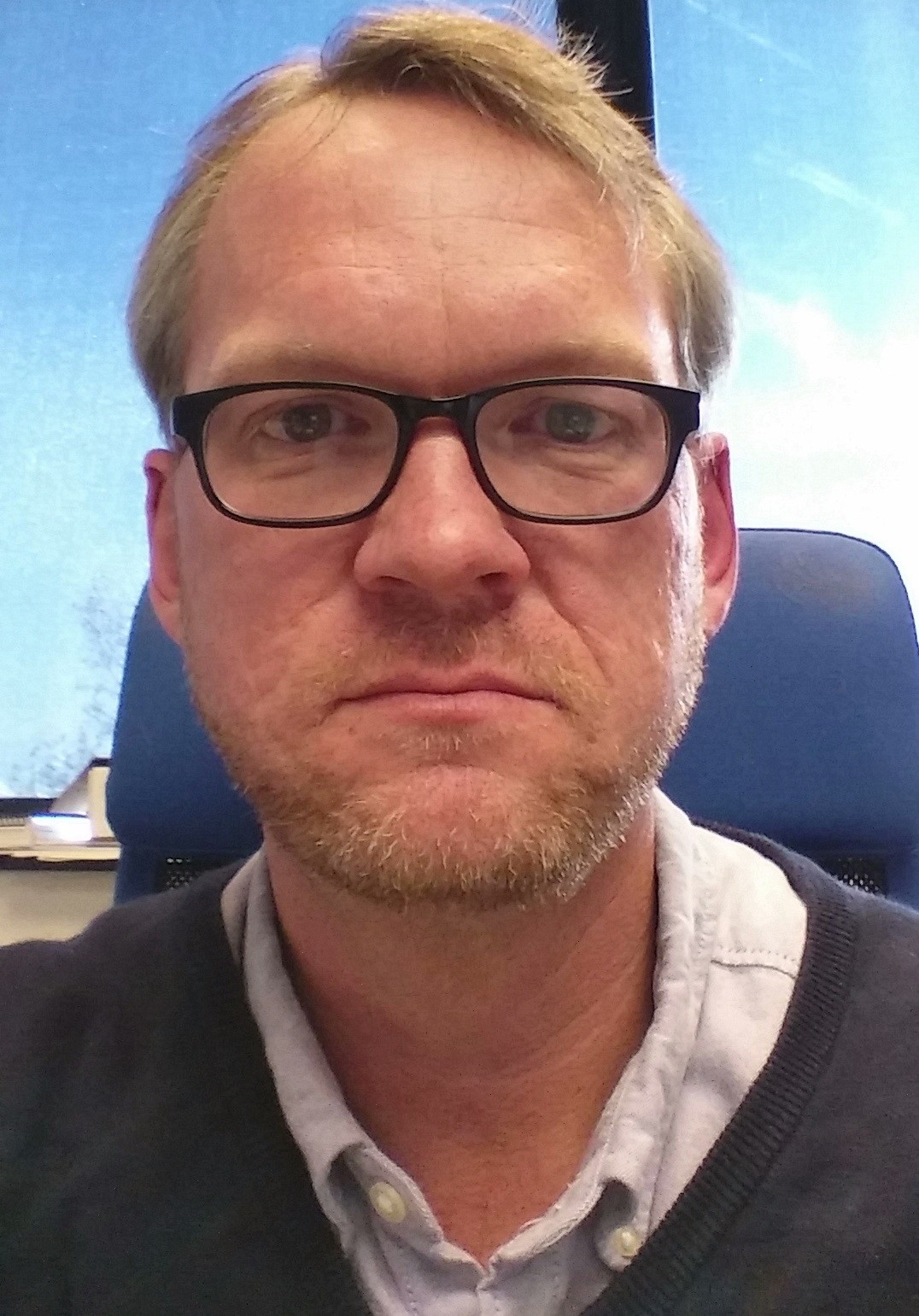
Prof. Aarno Parssinen
University of Oulu
Date:
Wednesday, Aug. 31st, 2:00pm-3:00pm
Location:
627 Mudd
|
New system concepts stretching the requirements of RFICs
Abstract:
Implementation constraints coming from RFIC technologies and other RF components set boundary conditions for new radio systems that try to stretch data rates, power consumption, cost and range to new extremes. Some of these techniques may be absolutely needed for optimal solutions but in many cases achieving sufficient performance in the extreme conditions may challenge research community for a long time. Requirements against RFIC solutions are evaluated using selected examples of existing wireless systems as well as looking forward to some of the key design aspects towards 5G.
Biography:
Aarno Parssinen received the M.Sc., Licentiate in Technology, and Doctor of Science degrees from the Helsinki University of Technology, Espoo, Finland, in 1995, 1997, and 2000, respectively, all in electrical engineering.
In 1996, he was a Research Visitor at the University of California at Santa Barbara. From 2000 to 2011, he was with Nokia Research Center, Helsinki, Finland. During 2009-2011, he served as a member of Nokia CEO Technology Council. From 2011 to 2013, he was with Renesas Mobile Corporation, Helsinki, working as a Distinguished Researcher and RF Research Manager. In 2013, as part of business acquisition, he joined Broadcom, Helsinki. Currently, he is a Professor at the University of Oulu, Finland.
His research interests include wireless systems and transceiver architectures for wireless communications, with special emphasis on the RF and analog integrated circuit and system design. He has authored and co-authored one book, one chapter of a book, and more than 50 international journal and conference papers, and he is the holder of several patents. He has served as a member of the Technical Program Committee of Int. Solid-State Circuits Conference since 2007, and he is currently the Chair of the Wireless Subcommittee. |
|
Prof. Jeffrey S. Walling
University of Utah
Date:
Friday, Oct. 14th, 2:00pm-3:00pm
Location:
414 CEPSR
|
Digital Transmitter Revolution: From Polar to Multiphase SCPAs
Abstract:
CMOS is ubiquitous for computation, and as such plays an ever increasing role in our lives as we use computation to improve working efficiency. Increasing levels of integration have made it possible to embed analog and RF circuits with digital processing to create RF systems-on-chip. The RF PA has been the exception to integration in CMOS, owing to relatively poor performance (e.g., low peak output power and low energy efficiency) when compared to other semiconductor technologies (e.g., III-V compounds, GaN and SiGe).
In this talk the switched capacitor PA (SCPAs) is introduced. It leverages CMOS inherent strengths of fast switching and lithographic matching to yield a linear, efficient digital PA. The original SCPA was a polar PA, subject to significant system level non-linearity (wide bandwidth, lack of synchronization, etc). I will introduce several techniques that implement SCPAs in discrete phase spaces; several multiple phase digital PA architectures will be discussed that alleviate the need for wideband phase modulators and synchronization. I will highlight several recent examples from the University of Utah PERFIC lab's research with applications of the multiphase techniques to the SCPA.
Biography:
Dr. Walling received the B.S. degree from the University of South Florida, Tampa, in 2000, and the M.S. and Ph. D. degrees from the University of Washington, Seattle, in 2005 and 2008, respectively. He was employed at Motorola, Plantation, FL working in cellular handset development. He interned for Intel from 2006-2007, working on highly-digital transmitters and CMOS PAs and continued this research while a Postdoctoral Researcher at the University of Washington. He is currently an assistant professor in the ECE department at University of Utah.
His current research focuses on high-efficiency digital transmitters for MIMO. Dr. Walling has authored ~50 journal articles conference papers and holds four patents. He received the Outstanding Teaching Award at University of Utah in 2015, the HKN Award for Excellence in Teaching in 2011, Best Paper Award at Mobicom 2012, the Yang Award for outstanding graduate research from the EE Department at University of Washington in 2008, an Intel Predoctoral Fellowship in 2007-2008, and the Analog Devices Outstanding Student Designer Award in 2006.
|
|
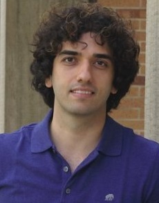
Prof. Tae-Hyoung Kim
Nanyang Technological University
Date:
Thursday, Nov. 17th, 3:00pm-4:00pm
Location:
EE Conf. Room, 13F Mudd
|
Ultra-low Power SRAM Design for Biomedical and IoT Applications
Abstract:
Recently, various ultra-low power applications such as wearable devices, biomedical devices and Internet-of-Things (IoT) have been developed opening up a new domain of integrated circuits design. In these applications, ultra-low power circuit techniques for improving the energy efficiency have been the main research focus. One of the most challenging blocks in ultra-low power systems is SRAM. A number of state-of-the-art circuit techniques have been proposed to tackle the ultra-low power SRAM design issues. In this talk, I will briefly explain various design issues in SRAM followed by various state-of-the-art design techniques. Some recent research works from my research group in NTU will also be introduced.
Biography:
Prof. Tae-Hyoung Kim received the B.S. and M.S. degrees in electrical engineering from Korea University, Seoul, Korea, in 1999 and 2001, respectively. He received the Ph.D. degree in electrical and computer engineering from University of Minnesota, Minneapolis, MN, USA in 2009. From 2001 to 2005, he worked for Samsung Electronics where he performed research on the design of high-speed SRAM memories, clock generators, and IO interface circuits. In 2007 ~ 2009 summer, he was with IBM T. J. Watson Research Center and Broadcom Corporation where he performed research on circuit reliability, low power SRAM, and battery backed memory design, respectively. On November 2009, he joined Nanyang Technological University as an assistant professor.
He received 2016 International Low Power Design Contest Award from ISLPED, a best paper award at 2014 and 2011 ISOCC, 2008 AMD/CICC Student Scholarship Award, 2008 Departmental Research Fellowship from Univ. of Minnesota, 2008 DAC/ISSCC Student Design Contest Award, 2008, 2001, and 1999 Samsung Humantec Thesis Award and, 2005 ETRI Journal Paper of the Year Award. He is an author/co-author of +100 journal and conference papers and has 17 US and Korean patents registered. His current research interests include low power and high performance digital, mixed-mode, and memory circuit design, ultra-low voltage circuits and systems design, variation and aging tolerant circuits and systems, and circuit techniques for 3D ICs. He serves as an associate editor of IEEE Transactions on VLSI Systems. He is an IEEE senior member and the Chair of IEEE Solid-State Circuits Society Singapore Chapter. He has served numerous conferences as a committee member.
|
|
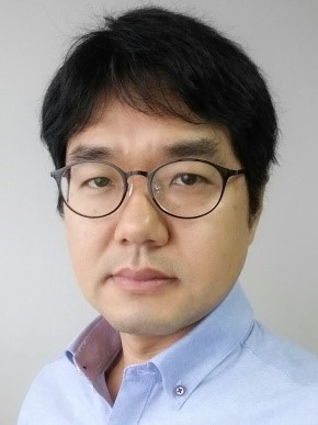
Dr. William Yee Li
Intel
Date:
Friday, Nov. 18th, 2:00pm-3:00pm
Location:
IAB 411
|
Analog/Mixed-Signal Circuit Design in Nanoscale CMOS
Abstract:
As CMOS technology scales, transistor density and speed increase resulting in more energy-efficient CPU and SOC. To interface among the powerful digital machines or with the physical world, analog/mixed-signal circuits play the critical role. However, aggressively scaled CMOS is not always analog friendly. To name a few but not all, the ever-decreasing voltage headroom, lower output impedance and higher variation seen in tiny transistors are undesirable characteristics. This talk will present several designs in phase-locked loop and temperature sensor in 22nm and 14nm, how design challenges are addressed and future directions.
Biography:
William Li received his Bachelor degree from The University of Hong Kong, M.S. and Ph.D. from Columbia University. He has been focusing on analog/mixed-signal circuit and system at Intel, conducting R&D in the latest process technologies in 65, 45, 32, 22, 14nm and beyond. His current research interests cover phase-locked loops, smart sensors, ADCs, and dc-dc converters.
|
|
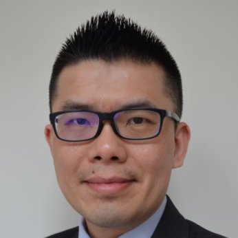
Dr. Shahriar Shahramian
Nokia-Bell Lab
Date:
Friday, Dec. 2nd, 2:00pm-3:00pm
Location:
414 CEPSR
|
Needle in a haystack - How to Find Hidden Parasitics in mm-Wave Layouts
Abstract:
This short course explores the hidden impairments which are often overlooked or difficult to locate in mm-Wave layouts and interconnects. Using real-life fabricated circuit blocks operating in the W-Band and optical circuits operating beyond 100Gb/s you are invited to search for parasitic capacitive, inductive and resistive elements which can adversely affect the circuit performance. After modeling of these elements, simulations demonstrate the impact of the parasitics on bandwidth, center frequency, stability and noise-figure. Using simple and quick modeling techniques the designers can incorporate various layout effects into their design.
Biography:
Shahriar Shahramian (M '06) received his Ph.D. degree from University of Toronto in 2010 where he focused on the design of mm-wave data converters and transceivers. Dr. Shahramian has been with the Bell Laboratories division of Alcatel-Lucent (now Nokia), Murray Hill, NJ since 2009 and is currently the Director of the mm-Wave ASIC Research Department. He is also a member of the technical program committee of Compound Semiconductor Integrated Circuit Symposium. His research focus includes the design of mm-wave wireless and wireline integrated circuits. He is the lead designer of several state-of-the-art ASICs for optical coherent and wireless backhaul product development at Bell Laboratories. Dr. Shahramian has been the recipient of Ontario Graduate Scholarship, University of Toronto Fellowship and the best paper award at the CSIC Symposium in 2005, 2015 and RFIC Symposium in 2015. He has also held an adjunct associate professor position at Columbia University, has received several teaching awards and is the founder and host of The Signal Path educational video series.
|
|
Fall 2016 Seminars
|
|
Title:
New system concepts stretching the requirements of RFICs
Speaker:
Prof. Aarno Parssinen
Date:
Wednesday, Aug. 31st, 2pm, 627 Mudd
Title:
Digital Transmitter Revolution: From Polar to Multiphase SCPAs
Speaker:
Prof. Jeffrey S. Walling
Date:
Friday, Oct. 14th, 2pm, 414 CEPSR
Title:
Ultra-low Power SRAM Design for Biomedical and IoT Applications
Speaker:
Prof. Tae-Hyoung Kim
Date:
Thursday, Nov. 17th, 3pm, EE Conf. Room, 13F Mudd
Title:
Analog/Mixed-Signal Circuit Design in Nanoscale CMOS
Speaker:
Dr. William Yee Li
Date:
Friday, Nov. 18th, 2pm, IAB 411
Title:
Needle in a haystack - How to Find Hidden Parasitics in mm-Wave Layouts
Speaker:
Dr. Shahriar Shahramian
Date:
Friday, Dec. 2nd, 2pm, 414 CEPSR
|
|
|
|
|