|
|
Fall 2013 Seminars
|
|
Title : A Model-Agnostic Technique for Simulating Per-Element Distortion Contributions
Speaker: Prof. Nagendra Krishnapura,
IIT Madras
Date: Thursday, Sep 26th, 4:10pm-5:10pm, 633 Mudd
Title : A Fully-Integrated Dual-Polarization 16-Element W-band Phased-Array Transceiver in SiGe BiCMOS
Speaker: Dr. Alberto Valdes-Garcia,
IBM T. J. Watson
Date: Friday, Oct 25th, 2:00pm-3:00pm, 825 Mudd
Title : Fully Integrated Phase Noise Extraction and Cancellation Technique for Ring-Oscillator Based Fractional-N PLLs
Speaker: Prof. Bertan Bakkaloglu,
ASU
Date: Wed, Nov 13th, 1:30pm-2:30pm, 227 Mudd
Title : Circuits and Architectures for Broadband Channelizers
Speaker: Prof. Ranjit Gharpurey,
UT-Austin
Date: Fri, Nov 15th, 11:10am-12:10pm, 627 Mudd
Title : Reconfigurable Radio-Frequency Transceivers (Distinguished Lecture Co-sponsored by IEEE NY EDS/SSCS)
Speaker: Prof. Hossein Hashemi,
USC
Date: Thursday, Nov 21st, 2:00pm-3:00pm, 253 Mudd (Engineering Terrace)
Title : Characterization of BTI induced variability in scaled Metal Gate / High-K CMOS technologies
Dr. Andreas Kerber,
GLOBALFOUNDRIES
Date: Friday, Dec 6th, 2:00pm-3:00pm, 825 Mudd
|
|
|
|

Prof. Nagendra Krishnapura,
IIT Madras
Date:
Thursday, Sep 26th, 4:10pm-5:10pm
Location:
633 Mudd
|
A Model-Agnostic Technique for Simulating Per-Element Distortion Contributions
Abstract:
The nonlinearity of an element can be altered while retaining the original operating point and first-order terms by appropriately combining multiple instances of the nonlinear element with appropriate scaling factors for incremental voltages above the operating points. Per-element distortion contributions in a circuit can then be determined by altering the nonlinear terms by known factors and simulating the output distortion in each case. This technique can be used in a standard circuit simulator with the appropriate nonlinear device models but requires no knowledge of the device model details on the part of the circuit designer. The technique is demonstrated by applying it to a common source amplifier with a nonlinear load and a two stage fully differential opamp.
Biography:
Prof. Nagendra Krishnapura obtained his BTech from the Indian Institute of Technology, Madras, India and his PhD from Columbia University, New York. He has worked as an analog design engineer at Texas Instruments, Bell Laboratories, Celight Inc., Multilink, and Vitesse semiconductor. He has taught analog circuit design courses at Columbia University as an adjunct faculty. He is currently an associate professor at the Indian Institute of Technology, Madras. His interests are analog and RF circuit design and analog signal processing.
|
|
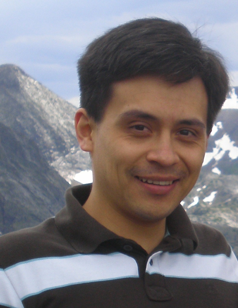
Dr. Alberto Valdes-Garcia,
IBM T. J. Watson
Date:
Friday, Oct 25th, 2:00pm-3:00pm
Location:
825 Mudd
|
A Fully-Integrated Dual-Polarization 16-Element W-band Phased-Array Transceiver in SiGe BiCMOS
Abstract:
This talk presents the design and measurement of a SiGe BiCMOS W-band (~94 GHz) phased-array transceiver IC with an in-package antenna array. The design targets radar and active imaging applications where light weight and low volume are important considerations; it also supports communication. By tiling an appropriate number of packaged ICs on a circuit board, any arbitrary antenna aperture can be realized, while maintaining ~λ/2 antenna element spacing. The IC integrates 32 receive elements and 16 transmit elements to support 16 dual polarized antennas in a package. It is fabricated in the IBM SiGe BiCMOS8HP 0.13um process, occupies an area of 6.6X6.7mm2, and operates from 2.7V (analog/RF) and 1.5V (digital) supplies. Measurement results show 8dB receiver NF and 2dBm transmitter output power per element at 94GHz in both polarizations.
Biography:
Dr. Alberto Valdes-Garcia is currently a Research Staff Member and Manager of the RF Circuits and Systems Group at the IBM T. J. Watson Research Center. He received the Ph.D. degree in Electrical Engineering from Texas A&M University in 2006. His present work is on silicon-integrated millimeter-wave systems and carbon electronics.
From 2006 to 2009, Dr. Valdes-Garcia served in the IEEE 802.15.3c 60GHz standardization committee. Since 2009 he serves as Technical Advisory Board member with Semiconductor Research Corporation (SRC), where he was Chair of the Integrated Circuits and Systems Sciences Coordinating Committee in 2011 and 2012. In spring 2013 he was also an Adjunct Assistant Professor at Columbia University. He holds 8 issued US patents with 25+ pending. His scholarly work (65+ authored or co-authored publications) has already received more than 1300+ independent citations in indexed journals. He is a co-Editor of the book 60GHz technology for Gbps WLAN and WPAN: From Theory to Practice (Wiley, 20011).
Dr. Valdes-Garcia is the winner of the 2005 Best Doctoral Thesis Award presented by the IEEE Test Technology Technical Council (TTTC), the recipient of the 2007 National Youth Award for Outstanding Academic Achievements, presented by the President of Mexico, and a co-recipient of the 2010 George Smith Award presented by the IEEE Electron Devices Society. In 2013, he was selected by the National Academy of Engineering for its Frontiers of Engineering Symposium.
|
|
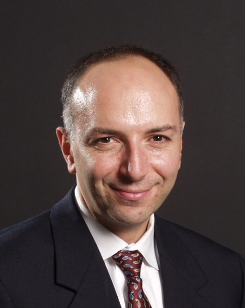
Prof. Bertan Bakkaloglu,
ASU
Date:
Wed, Nov 13th, 1:30pm-2:30pm
Location:
227 Mudd
|
Fully Integrated Phase Noise Extraction and Cancellation Technique for Ring-Oscillator Based Fractional-N PLLs
Abstract:
Ring-oscillators (ROs) provide a low-cost digital VCO solution in fully integrated PLLs. However due to their supply noise sensitivity and high noise floor, their applications have been limited to low performance applications. The proposed architecture introduces an analog feed-forward adaptive phase noise cancellation architecture that extracts and suppresses phase noise of ring-oscillators outside the PLL bandwidth. The proposed technique can improve the phase noise at an arbitrary offset frequency and bandwidth, and after initial calibration for gain it is insensitive to process, voltage and temperature variations. An experimental fractional PLL, with a loop bandwidth of 200 kHz is utilized to demonstrate the active phase noise cancellation approach. The cancellation loop is designed to suppress the phase noise at 1 MHz offset by 12.5 dB and reference spur by 13 dB with less than 17% increase in the overall power consumption at 5.1 GHz frequency. The measured phase noise at 1 MHz offset after cancellation is -105 dBc/Hz. The proposed RO-PLL is fabricated in 90nm CMOS process. With noise cancellation loop enabled, the PLL consumes 24.7 mA at 1.2V supply.
Biography:
Dr. Bakkaloglu received his PhD from Oregon State University in 1995 and joined Texas Instruments Inc. Mixed Signal Wireless Design Group, Dallas, TX, where he worked on analog, RF and mixed signal front ends for wireless and wireline communication ICs. He worked on system-on-chip designs with integrated battery management and RF, analog baseband functionality as a design leader. In 2004 he joined the Electrical Engineering Department at Arizona State University, Tempe, AZ, as an associate professor. His research interests include mixed signal circuit design for supply regulators, biomedical, chemical and MEMS sensor interface circuits, fractional-N frequency synthesizers, high speed data converters and built-in-self-diagnostic circuits for high reliability mixed signal circuits. Dr. Bakkaloglu has been associate editor for IEEE Transactions on Circuits and Systems and currently an associate editor for IEEE Transactions on Microwave Theory and Techniques. He is the Technical Program Committee Chair for 2014 RFIC Symposium.
|
|
Prof. Ranjit Gharpurey,
UT-Austin
Date:
Fri, Nov 15th, 11:10am-12:10pm
Location:
627 Mudd
|
Circuits and Architectures for Broadband Channelizers
Abstract:
Decomposing a broadband signal into multiple channels in the analog domain, for analysis, offers several potentially power-saving features compared to full-spectrum digitization, including the ability to selectively amplify, reject or digitize portions of the signal spectrum. In this talk we will describe circuits and architectures for broadband channelizers that perform analog-domain spectrum decomposition. Such channelizers can find application in cognitive radios, software-defined radios, spectrum analyzers and frequency-domain analog-to-digital converters. Key challenges and considerations in the design of such channelizers relating to LO synthesis, spurious performance and dynamic range will be addressed. Two architectures for broadband channelization will be described. The design of high performance harmonic rejection mixers employed in one of the approaches will be discussed. An architecture for feedback-based linearization of a channelizer will be presented. The talk will also provide a brief overview of other on-going work in our lab in the area of RF and high-speed analog circuit design.
Biography:
Ranjit Gharpurey is an Associate Professor in the Department of Electrical and Computer Engineering at the University of Texas at Austin. He received his B. Tech from the Indian Institute of Technology, Kharagpur, and his MS and PhD from the University of California at Berkeley. His current research includes RF and analog integrated circuit design, including topics relating to wireless ICs, interference detection and cancellation techniques, spectrum analysis, low-power design techniques, and high-efficiency baseband power amplifier topologies. Dr. Gharpurey has published extensively and has been awarded several patents in these areas. He has served as an Associate Editor of the IEEE Journal of Solid State Circuits, IEEE Transactions on Circuits and Systems, and a member of the program committees of CICC and ISSCC. He is currently on the TPC of ISQED and RFIC Symposium.
|
|
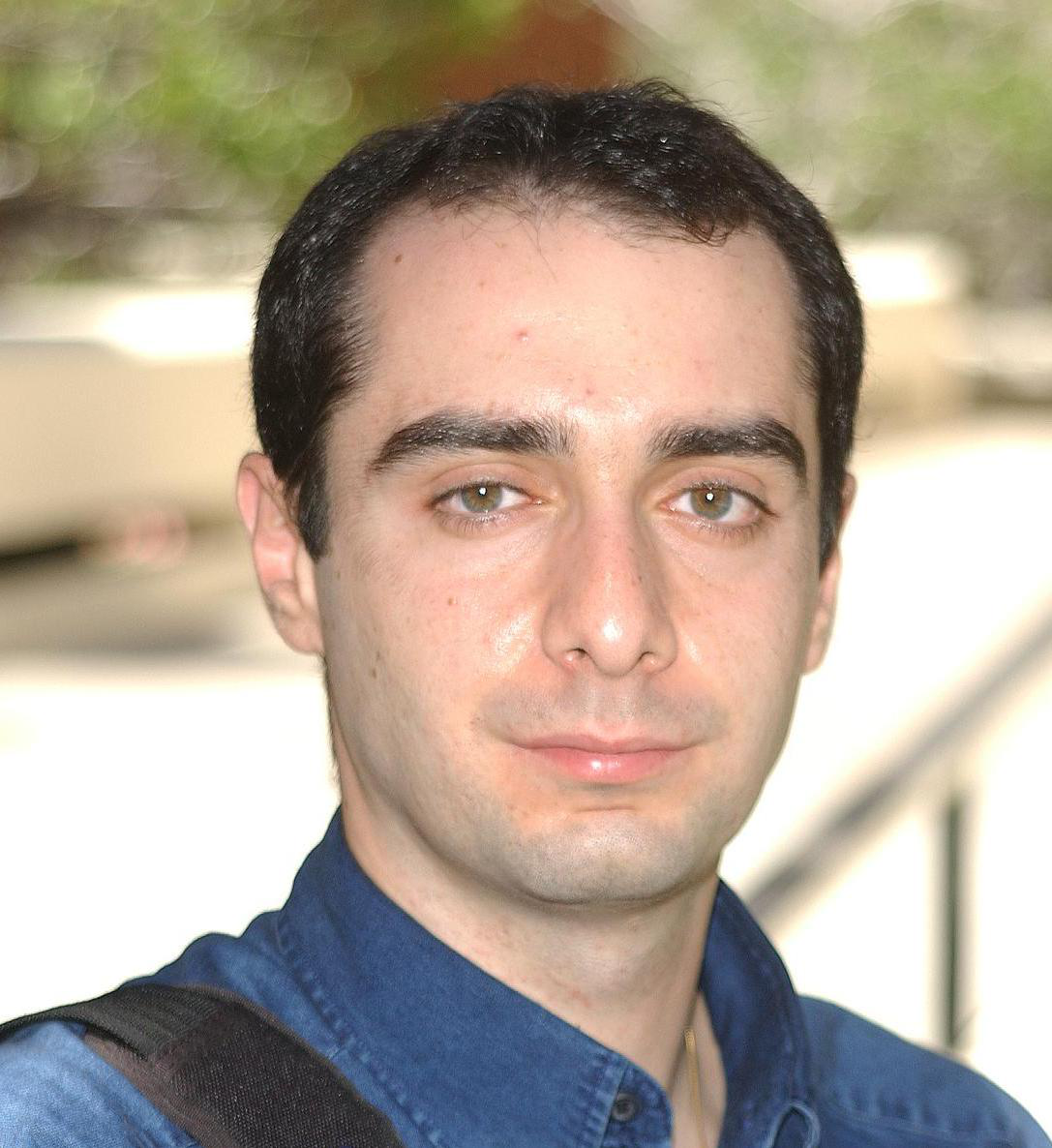
Prof. Hossein Hashemi,
USC
Date:
Thursday, Nov 21st, 2:00pm-3:00pm
Location:
253 Mudd (Engineering Terrace)
|
Reconfigurable Radio-Frequency Transceivers (Distinguished Lecture Co-sponsored by IEEE NY EDS/SSCS)
Abstract:
Modern commercial and military wireless systems should support various waveforms and standards under dynamically changing electromagnetic environments. A straight forward Software-Defined Radio (SDR) enables changing the radio parameters, such as carrier frequency, modulation format, and signal bandwidth, in a fixed architecture, through software. A more advanced reconfigurable radio enables changing the architecture of the transceiver and/or the individual building blocks in order to optimize the performance while minimizing the power consumption. Architectural level reconfigurability reduce the Non-Recurring Engineering (NRE) cost associated with the design of a new transceiver tailored to a specific application. Moreover, dynamic adjustment of radio architecture and specifications can be in response to, for instance, varying signal to noise ratio levels, locations and powers of interference and jamming signals, etc. This talk covers several examples of reconfigurable radio-frequency transceivers implemented in CMOS technology.
Biography:
Hossein Hashemi is an Associate Professor of Engineering, Ming Hsieh Faculty Fellow, and the co-director of the Ming Hsieh Institute and the Ultimate Radio Laboratory (UltRa-Lab) at the University of Southern California. He received the B.S. and M.S. degrees in Electronics Engineering from the Sharif University of Technology, Tehran, Iran, in 1997 and 1999, respectively, and the M.S. and Ph.D. degrees in Electrical Engineering from the California Institute of Technology, Pasadena, in 2001 and 2003, respectively. Dr. Hashemi currently serves on the Technical Program Committees of IEEE International Solid-State Circuits Conference (ISSCC), IEEE Radio Frequency Integrated Circuits (RFIC) Symposium, and the IEEE Compound Semiconductor Integrated Circuits Symposium (CSICS). He is also an Associate Editor for the IEEE Journal of Solid state Circuits (2013 - present), and Guest Editor of the same journal for October 2013 and December 2013 issues. He was an Associate Editor for the IEEE Transactions on Circuits and Systems-Part I: Regular Papers (2006-2007) and an Associate Editor for the IEEE Transactions on Circuits and Systems-Part II: Express Briefs (2004-2005). He was the recipient of the 2008 Defense Advanced Research Projects Agency (DARPA) Young Faculty Award and the National Science Foundation (NSF) CAREER Award. He received the USC Viterbi School of Engineering Junior Faculty Research Award in 2008, and was recognized as a Distinguished Scholar for the Outstanding Achievement in Advancement of Engineering by the Association of Professors and Scholars of Iranian Heritage in 2011. He was a co-recipient of the 2004 IEEE Journal of Solid-State Circuits Best Paper Award for 'A Fully-Integrated 24 GHz 8-Element Phased-Array Receiver in Silicon' and the 2007 IEEE International Solid-State Circuits Conference (ISSCC) Lewis Winner Award for Outstanding Paper for 'A Fully Integrated 24 GHz 4-Channel Phased-Array Transceiver in 0.13um CMOS based on a Variable Phase Ring Oscillator and PLL Architecture'. He is the co-editor of the book 'Millimeter-Wave Silicon Technology: 60 GHz and Beyond' published by Springer in 2008.
|
|
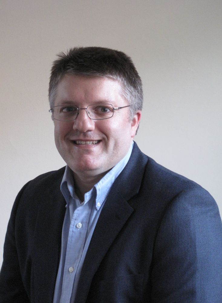
Dr. Andreas Kerber,
GLOBALFOUNDRIES
Date:
Friday, Dec 6th, 2:00pm-3:00pm
Location:
825 Mudd
|
Characterization of BTI induced variability in scaled Metal Gate / High-K CMOS technologies
Abstract:
Time-zero and time dependent variability is a growing concern for aggressively scaled transistor technologies with metal gate/high-k stacks. Bias temperature instability (BTI) in PMOS as well as NMOS devices is considered the most dominant time dependent variability component and needs to be modeled using stochastic processes. The physical nature of the stochastic process is still under debate and to support the model development efforts large statistical data sets are essential. In this presentation, we will focus on the characterization challenges related to stochastic BTI process in small area CMOS devices and discuss the large scale data we collected on discrete SRAM and logic devices. Finally we will elaborate on the impact of BTI induced variability on End-of-Life threshold voltage distributions and show that BTI induced variability is not the major contributing factor in the post stress threshold voltage variability in planar metal gate/high-k CMOS devices.
Biography:
Andreas Kerber was born in Schnann, Austria, and received his Diploma in physics from the University of Innsbruck, Austria, in 2001, during which time he was working at Bell Laboratories, Lucent Technologies (Murray Hill, NJ, USA) on the electrical characterization of ultra-thin gate oxides. In 2001, he joined Infineon Technologies in Munich, Germany. From 2001 to 2003, he was assigned to International SEMATECH at IMEC in Leuven, Belgium, where he was involved in the electrical characterization of alternative gate dielectrics for sub-100 nm CMOS technologies. At the same time he fulfilled the requirements for a PhD in electrical engineering and defended his thesis at the TU-Darmstadt, Germany, with honors. From 2004 to 2006, he was with the Reliability Methodology Department at Infineon Technologies in Munich, Germany, responsible for the dielectric reliability qualification of process technology transfers of 110 and 90 nm memory products. At the same time he developed a fast wafer-level data acquisition setup for time-dependent dielectric breakdown (TDDB) testing with sub-ms time resolution. In 2006, he joined AMD and now is with GLOBALFOUNDRIES in Yorktown Heights, NY, working as a Senior Member of Technical Staff on front-end-of-line (FEOL) reliability research with focus on metal gate / high-k CMOS process technology, advanced transistor architecture and device-to-circuit reliability correlation. Dr. Kerber has contributed to more than 80 journal and conference publications and presented his work at international conferences, including the VLSI Technology Symposium, the International Electron Device Meeting (IEDM) and the International Reliability Physics Symposium (IRPS). In addition, he has presented invited talks at the Workshop of Dielectrics in Microelectronics (WoDIM), the Semiconductor Interface Specialist Conference (SISC) and given tutorials on metal gate / high-k reliability characterization at the International Integrated Reliability Workshop (IIRW) and IRPS. Dr. Kerber has served as a technical program committee member for the SISC (2006, 2007), IRPS (2007, 2011, 2012), IEDM (2011, 2012) and Infos (2013).
|
|
|

